


Load Current (A)
Outp
u
t
Vo
lta
g
e
(V)
0
0.1
0.2
0.3
0.4
0.5
0.6
0.7
0.8
0.9
1
11.88
11.9
11.92
11.94
11.96
11.98
12
12.02
12.04
12.06
12.08
12.1
12.12
Ext-V
CC
FPWM = 1
VIN = 24 V
VIN = 48 V
VIN = 60 V
Input Voltage (V)
Ou
tp
u
t
V
o
lta
g
e
(V
)
15
20
25
30
35
40
45
50
55
60
11.88
11.9
11.92
11.94
11.96
11.98
12
12.02
12.04
12.06
12.08
12.1
12.12
Ext-V
CC
FPWM = 1
I
OUT
= 0 A
I
OUT
= 0.5 A
I
OUT
= 1 A
Typical Performance Curves
7
SNVU504A – August 2016 – Revised August 2016
Copyright © 2016, Texas Instruments Incorporated
LM5161 Buck EVM User’s Guide
When selecting the FPWM mode, the LM5161 needs an external feedback ripple injection circuit (Type 3)
or
the external ESR resistor (Type 1) on board, for normal operation. The correct values for the external
ESR resistor (R4 in the EVM) in series with the output capacitors (C10, C11) or for the external ripple
injection circuit (R6,C7 and C10), depending on which ripple injection scheme (Type 1 or Type 3) is used,
are calculated based on the formulae mentioned in the
datasheet. See application note
for more details for each ripple generation method.
When selecting the DCM mode setting using the Jumper (
JP1
) see
, the internal emulated ripple
mode is enabled. When operating in this mode, there is no need to add the external ESR resistor in series
with the output capacitors or the external ripple injection circuit (see
for more details). The
internal emulated ripple is sufficient to maintain steady-state and dynamic stability while operating in this
mode. In a typical buck application at T
J
> 125°C and FPWM = 0, with the input voltage VIN > 72 V and
the V
CC
externally supplied add a BST resistor, R2 (recommended > 3
Ω
) in series with the BST capacitor
(see
). This protects the internal bootstrap diode during a full load transient operation.
An external voltage can be supplied to the VCC pin in the range of 9 V to 13 V, for improved efficiency
requirements. In that case, the diode D1 must be appropriately populated. The user can keep diode D1
populated on board and install/uninstall the jumper
J4
in order to estimate the difference in efficiency, with
and without the external V
CC
supply. More details about the diode D1 are given in the
Table 2. FPWM Pin Mode
JP1 Setting
Logic Stage
Description
DCM or Floating (High Z) (Pin 2 - Pin 3:
DCM)
0
The FPWM pin is grounded or left floating. Populate
resistor R2 appropriately. DCM with the pulse
skipping mode at light load enabled. No external
ripple injection circuit needed.
FPWM (VCC) (Pin 2 - Pin 1: FPWM)
1
The FPWM pin is connected to VCC. External Ripple
Injection circuit needed. CCM mode enabled over the
entire load range.
4
Typical Performance Curves
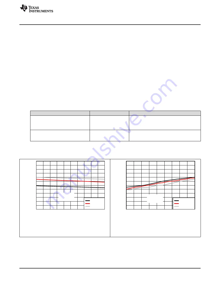
V
OUT
- V
CC
diode
connected
FPWM = 1
F
SW
= 300kHz
Figure 2. Load Regulation
V
OUT
- V
CC
diode
connected
FPWM = 1
F
SW
= 300kHz
Figure 3. Line Regulation