background image

2 Application Schematic

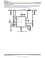
The LM5157EVM-BST is capable of multiple configurations. 

Figure 2-1

 shows the standard configuration of the 

LM5157EVM-BST for which the parameters in 

Table 1-1

 are valid. 

Section 4.2

 describes the correct jumper 

settings and measurement locations to recreate the data presented in 

Section 5

.

VCC

BIAS

UVLO/SYNC

AGND

PGOOD

RT

SS

SW

PGND

FB

COMP

MODE

VCC

VCC

V

SUPPLY

V

LOAD

L

M

D

LM5157

R

FBT

R

FBB

C

HF

C

COMP

R

COMP

C

SS

C

VCC

R

PG

C

OUT

R

UVB

R

UVT

C

IN

R

FREQ

R

MODE

Figure 2-1. Application Circuit

www.ti.com

Application Schematic

SNVU739A – OCTOBER 2020 – REVISED AUGUST 2021

Submit Document Feedback

LM5157EVM-BST Evaluation Module

5

Copyright © 2021 Texas Instruments Incorporated

Summary of Contents for LM5157EVM-BST

Page 1: ...V IOUT 1 6 A VBIAS VIN no Forced Air Cooling 9 Figure 5 7 Steady State VIN 3 V IOUT 0 6 A 10 Figure 5 8 Steady State VIN 6 V IOUT 1 6 A 10 Figure 5 9 Steady State VIN 9 V IOUT 1 6 A 10 Figure 5 10 Start Up VIN 3 V IOUT 0 6 A 20 Ω 11 Figure 5 11 Start Up VIN 6 V IOUT 1 6 A 7 5 Ω 11 Figure 5 12 Start Up VIN 9 V IOUT 1 6 A 7 5 Ω 11 Figure 5 13 Load Transient VIN 3 V IOUT 0 3 A to 0 6 A 12 Figure 5 14...

Page 2: ... 16 Trademarks All trademarks are the property of their respective owners Trademarks www ti com 2 LM5157EVM BST Evaluation Module SNVU739A OCTOBER 2020 REVISED AUGUST 2021 Submit Document Feedback Copyright 2021 Texas Instruments Incorporated ...
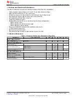
Page 3: ...th selectable pullup source 2 1 MHz switching frequency External clock synchronization Programmable dual random spread spectrum reduces the EMI 1 1 Electrical Parameters Table 1 1 Electrical Performance Standard Configuration PARAMETER TEST CONDITIONS MIN TYP MAX UNIT INPUT CHARACTERISTICS Input voltage range VIN Operation 3 6 9 V OUTPUT CHARACTERISTICS Output Voltage VOUT 12 V Maximum output curr...

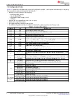
Page 4: ... TP11 SD High signal pulls the UVLO pin to ground entering shutdown mode TP12 AGND Negative input of external signals J6 Pin 1 to pin 2 Connect VOUT to the BIAS pin of the LM5157 through D2 only set one jumper to J6 J7 J8 or J9 Pin 2 to pin 3 Directly connect VOUT to the BIAS pin of the LM5157 only set one jumper to J6 J7 J8 or J9 J7 Pin 1 to pin 2 Connect VIN to the BIAS pin of the LM5157 through...

Page 5: ...s and measurement locations to recreate the data presented in Section 5 VCC BIAS UVLO SYNC AGND PGOOD RT SS SW PGND FB COMP MODE VCC VCC VSUPPLY VLOAD LM D LM5157 RFBT RFBB CHF CCOMP RCOMP CSS CVCC RPG COUT RUVB RUVT CIN RFREQ RMODE Figure 2 1 Application Circuit www ti com Application Schematic SNVU739A OCTOBER 2020 REVISED AUGUST 2021 Submit Document Feedback LM5157EVM BST Evaluation Module 5 Co...

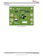
Page 6: ...ture of the LM5157EVM BST The actual board color can differ Figure 3 1 EVM Picture EVM Picture www ti com 6 LM5157EVM BST Evaluation Module SNVU739A OCTOBER 2020 REVISED AUGUST 2021 Submit Document Feedback Copyright 2021 Texas Instruments Incorporated ...
Page 7: ...age connect from VIN to GND Voltmeter 2 Output voltage connect from VOUT to GND Ammeter 1 Input current must be able to handle 10 A Shunt resistor can be used as needed Ammeter 2 Output current must be able to handle 2 A Shunt resistor can be used as needed Electronic Load The load should be constant resistance CR or constant current CC capable It should safely handle 2 A at 12 V Oscilloscope 20 M...

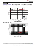
Page 8: ... Efficiency 0 0 2 0 4 0 6 0 8 1 1 2 1 4 1 6 1 8 2 0 20 40 60 80 100 VIN 3 V VIN 4 V VIN 6 V VIN 9 V Figure 5 1 Efficiency vs Load 5 2 Load Regulation Curve IOUT A V OUT V 0 0 2 0 4 0 6 0 8 1 1 2 1 4 1 6 1 8 2 11 88 11 9 11 92 11 94 11 96 11 98 12 12 02 12 04 12 06 12 08 12 1 12 12 VIN 3 V VIN 4 V VIN 6 V VIN 9 V Figure 5 2 Load Regulation Test Results www ti com 8 LM5157EVM BST Evaluation Module S...

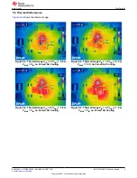
Page 9: ...V IOUT 0 6 A VBIAS 12 V no Forced Air Cooling Figure 5 5 Thermal Image VIN 6 V IOUT 1 6 A VBIAS VIN no Forced Air Cooling Figure 5 6 Thermal Image VIN 9 V IOUT 1 6 A VBIAS VIN no Forced Air Cooling www ti com Test Results SNVU739A OCTOBER 2020 REVISED AUGUST 2021 Submit Document Feedback LM5157EVM BST Evaluation Module 9 Copyright 2021 Texas Instruments Incorporated ...
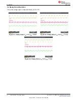
Page 10: ... 5 7 Steady State VIN 3 V IOUT 0 6 A Figure 5 8 Steady State VIN 6 V IOUT 1 6 A Figure 5 9 Steady State VIN 9 V IOUT 1 6 A Test Results www ti com 10 LM5157EVM BST Evaluation Module SNVU739A OCTOBER 2020 REVISED AUGUST 2021 Submit Document Feedback Copyright 2021 Texas Instruments Incorporated ...
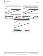
Page 11: ... Ω Figure 5 11 Start Up VIN 6 V IOUT 1 6 A 7 5 Ω Figure 5 12 Start Up VIN 9 V IOUT 1 6 A 7 5 Ω www ti com Test Results SNVU739A OCTOBER 2020 REVISED AUGUST 2021 Submit Document Feedback LM5157EVM BST Evaluation Module 11 Copyright 2021 Texas Instruments Incorporated ...

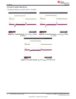
Page 12: ...VIN 3 V IOUT 0 3 A to 0 6 A Figure 5 14 Load Transient VIN 6 V IOUT 0 8 A to 1 6 A Figure 5 15 Load Transient VIN 9 V IOUT 0 8 A to 1 6 A Test Results www ti com 12 LM5157EVM BST Evaluation Module SNVU739A OCTOBER 2020 REVISED AUGUST 2021 Submit Document Feedback Copyright 2021 Texas Instruments Incorporated ...
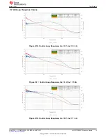
Page 13: ... A Figure 5 17 Control Loop Response VIN 6 V IOUT 1 6A Figure 5 18 Control Loop Response VIN 9 V IOUT 1 6 A www ti com Test Results SNVU739A OCTOBER 2020 REVISED AUGUST 2021 Submit Document Feedback LM5157EVM BST Evaluation Module 13 Copyright 2021 Texas Instruments Incorporated ...
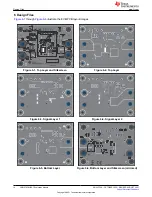
Page 14: ...n Figure 6 2 Top Layer Figure 6 3 Signal Layer 1 Figure 6 4 Signal Layer 2 Figure 6 5 Bottom Layer Figure 6 6 Bottom Layer and Silkscreen mirrored Design Files www ti com 14 LM5157EVM BST Evaluation Module SNVU739A OCTOBER 2020 REVISED AUGUST 2021 Submit Document Feedback Copyright 2021 Texas Instruments Incorporated ...
Page 15: ...15 PGND 16 PGND 1 VCC 2 BIAS 3 PGOOD 4 RT 5 EN UVLO SYNC 6 AGND 7 SS 10 COMP 8 FB 9 MODE 11 SW 12 SW 13 SW 14 EP 17 LM5157QRTERQ1 U1 VCC VAUX PGOOD 100k R10 100k R11 PGND AGND NT1 Net Tie 1 3 2 45V D1 AGND AGND 1nF C23 FB FB 1 6A 0 8A 4 7uF C13 4 7uF C14 4 7uF C15 4 7uF C16 4 7uF C17 4 7uF C18 100pF C27 22nF C25 9 53k R14 71 5k R12 61 9k R5 1 6A 0 8A LM5157EVM BST 2 61k R19 10nF C26 100uF C11 100u...

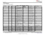
Page 16: ...188R72A104KA01D MuRata C25 1 0 022 μF CAP CERM 0 022 μF 50 V 10 X7R 0603 603 C0603X223K5RACTU Kemet C27 1 100 pF CAP CERM 100 pF 50 V 5 C0G NP0 AEC Q200 Grade 0 0603 603 CGA3E2NP01H101J080AA TDK D1 1 45 V Diode Schottky 45 V 10 A AEC Q101 CFP15 CFP15 PMEG045V100EPDAZ Nexperia D2 D3 2 60 V Diode Schottky 60 V 1 A SOD 123F SOD 123F PMEG6010CEH 115 Nexperia L2 1 1 5 μH Inductor Shielded Composite 1 5...

Page 17: ...53L Yageo R16 1 37 4 k RES 37 4 k 1 0 1 W 0603 603 RC0603FR 0737K4L Yageo R17 1 10 0 k RES 10 0 k 1 0 1 W 0603 603 RC0603FR 0710KL Yageo R18 1 62 0 k RES 62 0 k 1 0 1 W 0603 603 RC0603FR 0762KL Yageo R19 1 2 61 k RES 2 61 k 1 0 1 W 0603 603 RC0603FR 072K61L Yageo U1 1 2 2 MHz Wide VIN Boost Sepic Flyback Converter with Dual Random Spread Spectrum RTE0016K WQFN 16 RTE0016K LM5157QRTERQ1 Texas Instr...

Page 18: ...ctober 2020 to Revision A August 2021 Page Updated all measurements 1 Added resistor in series to the VCC capacitor 1 Updated Figure 6 7 15 Updated Table 6 1 16 Revision History www ti com 18 LM5157EVM BST Evaluation Module SNVU739A OCTOBER 2020 REVISED AUGUST 2021 Submit Document Feedback Copyright 2021 Texas Instruments Incorporated ...
Page 19: ...other than TI b the nonconformity resulted from User s design specifications or instructions for such EVMs or improper system design or c User has not paid on time Testing and other quality control techniques are used to the extent TI deems necessary TI does not test all parameters of each EVM User s claims against TI under this Section 2 are void if User fails to notify TI of any apparent defects...

Page 20: ... These limits are designed to provide reasonable protection against harmful interference in a residential installation This equipment generates uses and can radiate radio frequency energy and if not installed and used in accordance with the instructions may cause harmful interference to radio communications However there is no guarantee that interference will not occur in a particular installation...

Page 21: ...y for convenience and should be verified by User 1 Use EVMs in a shielded room or any other test facility as defined in the notification 173 issued by Ministry of Internal Affairs and Communications on March 28 2006 based on Sub section 1 1 of Article 6 of the Ministry s Rule for Enforcement of Radio Law of Japan 2 Use EVMs only after User obtains the license of Test Radio Station as provided in R...

Page 22: ... any interfaces electronic and or mechanical between the EVM and any human body are designed with suitable isolation and means to safely limit accessible leakage currents to minimize the risk of electrical shock hazard User assumes all responsibility and liability for any improper or unsafe handling or use of the EVM by User or its employees affiliates contractors or designees 4 4 User assumes all...

Page 23: ...OR DAMAGES ARE CLAIMED THE EXISTENCE OF MORE THAN ONE CLAIM SHALL NOT ENLARGE OR EXTEND THIS LIMIT 9 Return Policy Except as otherwise provided TI does not offer any refunds returns or exchanges Furthermore no return of EVM s will be accepted if the package has been opened and no return of the EVM s will be accepted if they are damaged or otherwise not in a resalable condition If User feels it has...

Page 24: ...s are subject to change without notice TI grants you permission to use these resources only for development of an application that uses the TI products described in the resource Other reproduction and display of these resources is prohibited No license is granted to any other TI intellectual property right or to any third party intellectual property right TI disclaims responsibility for and you wi...

Reviews: