


OUT0
Pin
INTB
Pin
25 ms scan cycle
25 ms scan cycle
Sampling
25 ms scan cycle
Sampling
Reading the Status
Register clears the
OUT_STATUS bit.
Sampling
Button 0
pressed
Button 0
released
OUT0 de-asserted
STATUS
Register
OUT
n
DQG ,17% DUH SURJUDPPHG WR ³$FWLYH /RZ´
. Scan Rate: 40 SPS.
Events
OUT0 and
INTB asserted,
OUT_STATUS
bit asserted
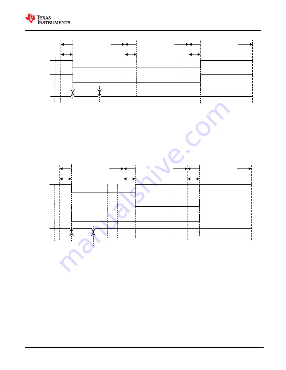
Figure 8-13. Timing Diagram of a Single Button Press
shows the LDC3114 response to multiple button presses. In this example, after Button 0 is pressed,
the OUT0 pin is asserted. After that, Button 1 is also pressed, following which Button 0 is released. The OUT0
pin is de-asserted and OUT1 pin asserted at the end of the next button sampling window. The INTB pin remains
continuously asserted as long as at least one of the buttons is pressed. The OUT_STATUS bit only changes
from 0 to 1 after the first button assertion.
OUT0
Pin
INTB
Pin
25 ms scan cycle
25 ms scan cycle
Sampling
25 ms scan cycle
Sampling
Sampling
OUT0 and
INTB asserted
OUT0 de-asserted
OUT1 asserted
STATUS
Register
OUT1
Pin
Button 0
pressed
Button 1
released
OUT1 and INTB
de-asserted
Button 1
pressed
Button 0
released
Reading the Status Register
clears the OUT_STATUS bit.
OUT
n
DQG ,17% DUH SURJUDPPHG WR ³$FWLYH /RZ´
. Scan Rate: 40 SPS.
Events
Figure 8-14. Timing Diagram of Multiple Button Presses
The INTB pin also reports any error event. If an error occurs, the INTB pin is asserted and the error is reported in
the STATUS register (Address 0x00). Refer to the
section for possible error events.
For Raw data access mode, the OUTx pins are not used and INTB pin along with error is also used to assert
when the sampling cycle is complete and data is available for all channels.
SNOSDD0 – DECEMBER 2021
Copyright © 2021 Texas Instruments Incorporated
47


