


10µF
C1
0.1µF
C2
IN
1
OUT
5
2
CBYP
4
ON/OFF
3
GND
REG1
2.2µF
C3
1µF
C5
VM
GND
GND
IN1
IN2
GND
VM
GND
IN1X
IN1
IN2X
IN2
V
M
0.1µF
C6
VCCX
VCC
GND
0.01µF
C4
VM
1
OUT1
2
OUT2
3
GND
4
IN2
5
IN1
6
SLEEP
7
VCC
8
PAD
9
U1
DRV8837CDSG
JP1
GND
VCC
IN1
IN2
VCC
VM
0
R1
0
R2
0
R3
TP1
TP2
TP3
TP4
D1
100
R4
GND
GND
1
2
3
JP2
JP3
P1.0/TA0CLK/ACLK/A0
1
P1.1/TA0.0/A1
2
P1.2/TA0.1/A2
3
P1.3/ADC10CLK/A3/VREF-/VEREF-
4
P1.4/SMCLK/A4/VREF+/VEREF+/TCK
5
P1.5/TA0.0/A5/SCLK/TMS
6
P1.6/TA0.1/A6/SDO/SCL/TDI/TCLK
7
P1.7/A7/SDI/SDA/TDO/TDI
8
RST/NMI/SBWTDIO
9
TEST/SBWTCK
10
P2.7/XOUT
11
P2.6/XIN/TA0.1
12
DVSS
13
DVSS
14
DVCC
15
DVCC
16
PAD
17
U2
MSP430G2131IRSA16R
1
2
3
4
J1
GND
GND
TEST
RESET
TEST
RESET
SPEED REF
IN1X
DIR
VREF
P1.5
P1.6
P1.7
IN2X
P2.7
47k
R5
0.1µF
C7
GND
JP4
1.0k
R6
GND
VCC
DIR
10k ohm
R7
VREF
SPEED REF
GND
DI
R
SPE
ED
RE
F
TP5
TP6
VBUS
1
D-
2
D+
3
ID
4
GND
5
6
7
8
1
1
10
9
J2
0473460001
GND
GND
VM
VCC
VCCX
D2
STATUS
VCC
STATUS
GND
Remove these resistors if supplying
external signals to the motor driver.
Copyright © 2016, Texas Instruments Incorporated
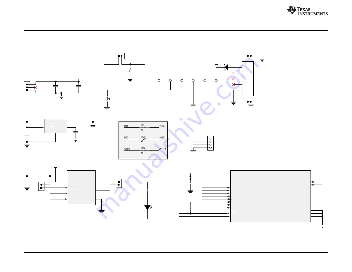
DRV8837CEVM Schematic
6
SLVUAS3 – June 2016
Copyright © 2016, Texas Instruments Incorporated
DRV8837C Evaluation Module User's Guide
5
DRV8837CEVM Schematic
shows the DRV8837CEVM schematic.
Figure 3. DRV8837CEVM Schematic