


n
S
L
E
E
P
A
O
U
T
1
AISEN
AOUT2
BOUT2
BISEN
B
O
U
T
1
n
F
A
U
L
T
B
IN
1
B
IN
2
NC
VM
GND
VINT
A
IN
2
A
IN
1
(PPAD)
U1
DRV8833C
DVCC
1
P1.0/TA0CLK/ACLK/A0/CA0
2
P1.1/TA0.0/UCA0RXD/UCA0SOMI/A1/CA1
3
P1.2/TA0.1/UCA0TXD/PUCA0SIMO/A2/CA2
4
P1.3/ADC10CLK/CAOUT/VREF-/A3/CA3
5
P1.4/SMCLK/UCB0STE/UCA0CLK/VREF+
6
P1.5/TA0.0/UCB0CLK/A5/CA5
7
P2.0/TA1.0
8
P2.1/TA1.1
9
P2.2/TA1.1
10
P2.3/TA1.0
11
P2.4/TA1.2
12
P2.5/TA1.2
13
P1.6/TA0.1/UCB0SOMI/UCB0SCL/A6/CA6
14
P1.7/UCB0SIMO/UCBSDA/A7/CA7
15
RST/NMI/SBWTDIO
16
TEST/SBWTCK
17
XOUT/P2.7
18
XIN/P2.6/TA0.1
19
DVSS
20
U2
MSP430G2553IPW20
1
2
3
4
J2
Spy-Bi-Wire
47k
R1
1nF
C4
S
p
ee
d
d
o
w
n
V3P3
1µF
C3
2.2µF
C6
1.0
R
2
1.0
R
3
1.0
R
4
1.0
R
5
1.0
R
6
1.0
R
7
AOUT1
AOUT2
BOUT2
BOUT1
AISEN
BISEN
1
2
nSLEEP
V3P3
V3P3
390
R10
10k
R9
C
1
A
2
D2
nFAULT
390
R8
C
1
A
2
D1
STATE
2.2µF
C2
1µF
C1
1
2
3
4
J7
1
2
J5
ED555/2DS
1
2
J8
ED555/2DS
AOUT1
AOUT2
BOUT2
BOUT1
AOUT1
AOUT2
BOUT2
BOUT1
VM
BOUT1
BOUT2
AOUT2
AOUT1
V3P3
VM
BISEN
AISEN
1
2
3
4
5
J4
1
2
DIR
1
2
Full/Half
Notes: 1) For normal operation, populate resistor packs R11
2) For external control, remove resistor packs R11, and provide signals at J4
3) Signals can be observed at J4 during normal operation
Stepper motor connector
VM input connector (4V to 10.8V)
IN
1
OUT
5
2
CBYP
4
ON/OFF
3
GND
U4
LP2985
1
2
3
4
5
6
7
8
9
10
11
12
13
14
15
16
R11
EXB-2HV330JV
RST
2
G
N
D
1
VDD
3
U3
TLV 803DBZ
0.01µF
C7
VM
V3P3
VM to 3.3V LDO
V3P3
RST
RST
3.3V monitor
1
2
3
4
5
6
J1
1
2
3
4
5
6
J3
nFAULT
AIN1
AIN2
BIN2
BIN1
P1.0
P1.1
P1.2
P1.3
P1.0
P1.1
P1.2
P1.3
MSP430G2553 Unit
nFAULT LED
AIN1
AIN2
BIN2
BIN1
22µF
C5
DRV8833C Unit
B
IS
E
N
A
IS
E
N
Current sense resistors
AOUT2
BOUT2
AOUT1
BOUT1
BISEN
AISEN
V3P3
VM
Test points
Control signal bridge
VM
Connect 1 Jumper for 200mA
Ichop = 0.2V/RSENSE
(Note: In most of cases, C5=10uF will be fine with motor load < 10W)
1
2
J6
ED555/2DS
GND1
GND
1
GND
2
GND2
VINT
VINT
VINT
S
p
ee
d
u
p
S
ta
rt
/S
to
p
Connect 2 Jumpers for 400mA
Connect 3 Jumpers for 600mA
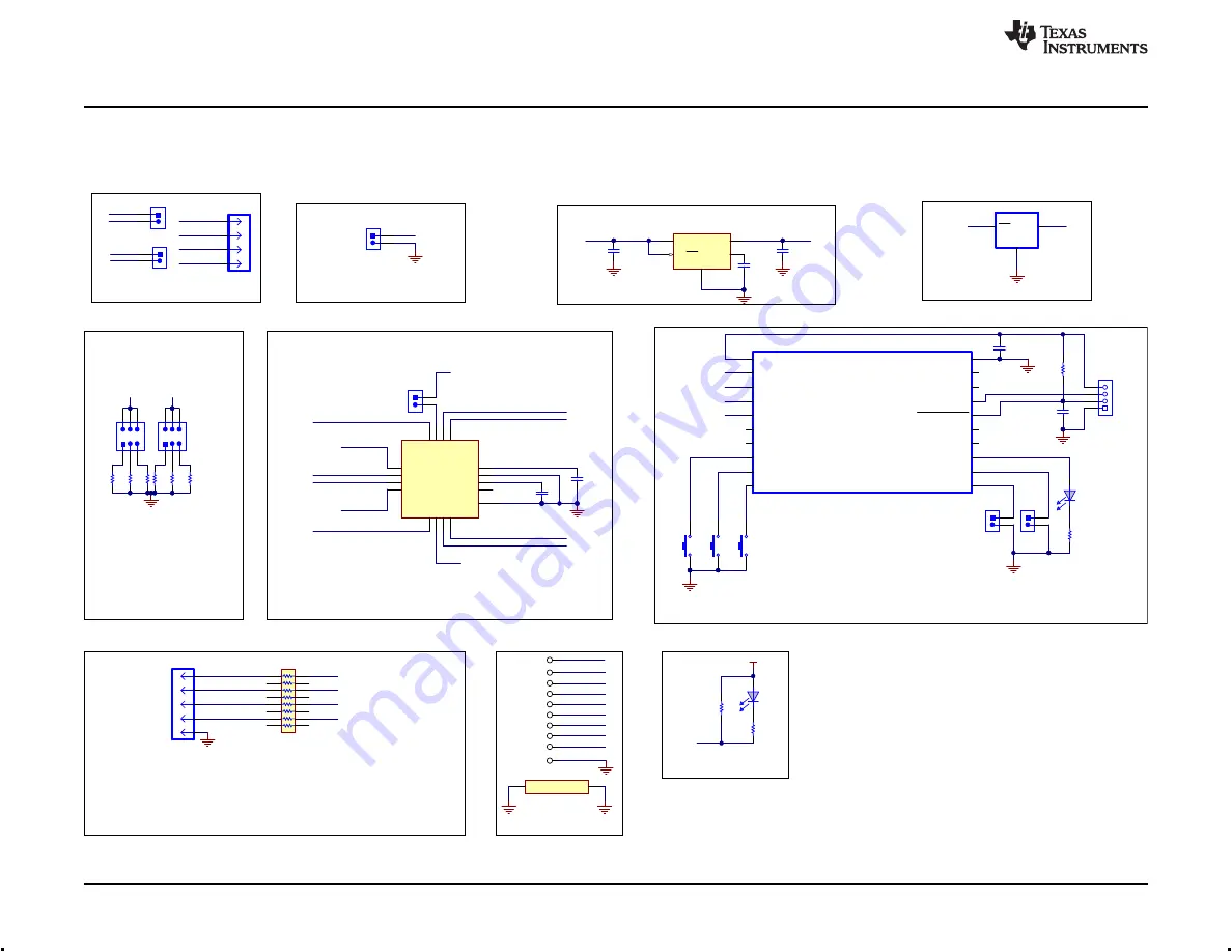
Schematic
3
Schematic
The schematic (
) in this document may be less resolution ratio. Refer to the separately provided schematic file in the EVM reference
package.
Figure 5. EVM Schematic
6
DRV8833C Evaluation Module
SLVUAD4 – November 2014
Copyright © 2014, Texas Instruments Incorporated


