background image

www.ti.com

Quick Start Guide

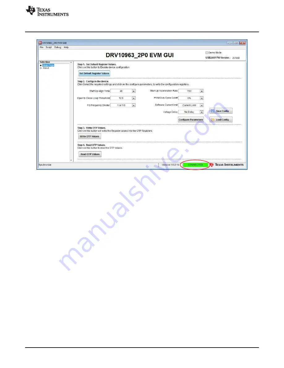
Figure 5. GUI Screen With Successful I2C Interface

3. Left-click on the step 1 button “Set Default Resister Values”. Step 1 is always mandatory before

proceeding to step 2 to enable configuration of the device. This step programs the following
parameters to the corresponding shadow register, as shown in

Figure 6

. These default values

correspond to the factory programmed part DRV10963JJ. Refer to the DRV10963 datasheet for a
detailed explanation of different versions of DRV10963 and descriptions of tunable parameters.

"Start Up Align Time" - 350 ms and "Start-up Acceleration Rate" - 80 Hz/s

"Open to Close Loop Threshold" - 100 Hz

"PWM Duty Cycle Cutoff" - 10%

"FG Frequency Divider" - 1 or 1/3

"Software Current limit" - 500 mA

"Voltage Delay" - 120 µs

To enable motor spin with the above parameters, open the jumper J1 on the motherboard. There is a
high probability that the motor will start rotating with previously shown default values. This state is
equivalent to driving the motor at maximum speed with 100% duty cycle because PWM input being
connected to the I

2

C clock input continues to receive a high signal. Ensure that the parameters

previously shown are optimized for their end application. Refer to

Section 6

for guidelines to optimally

determine and tune motor parameters using the GUI.

9

SLAU643 – July 2015

DRV10963 Evaluation Module

Submit Documentation Feedback

Copyright © 2015, Texas Instruments Incorporated

Summary of Contents for DRV10963

Page 1: ...EVM 7 5 5 Tuning GUI to Configure Motor Parameter 8 6 Tuning Guide 13 6 1 Configuring the Device 13 6 2 Writing to the OTP Registers 16 6 3 Reading the OTP Values 18 6 4 Notes 18 7 Schematic and Bill...

Page 2: ...5 4 Connector P2 Motherboard 5 5 DRV10963 Motherboard Bill of Materials 22 6 DRV10963 Daughterboard Bill of Materials 23 1 DRV10963 EVM Kit Contents The DRV10963 evaluation kit contains following 1 DR...

Page 3: ...device OTP The DRV10963 EVM comes with blank version device with un programmed OTP bits The DRV10963 device has configurable shadow registers corresponding to each OTP bit Shadow registers provide ea...

Page 4: ...are used to interface the daughter socket board The pin assignments are as follows Table 1 Connector P1 Daughterboard Pin Description 1 2 NC 3 FR Dual functionality 1 Forward reverse for motor directi...

Page 5: ...on 1 U 2 W 3 V 4 2 Interface Connectors to Motherboard P1 P2 Connectors P1 P2 are used to interface signals coming from the motherboard to the device via socket The pin assignments are as follows Tabl...

Page 6: ...om download labview run time engine 2014 4887 en CAUTION Do not apply power to board before you have verified settings mentioned in Section 5 2 and Section 5 3 5 2 Initial Hardware Settings The kit sh...

Page 7: ...to establish a successful connection with the GUI 1 Do not power up the power supply First connect the power supply ground to pin GND the 6 2 V to pin V_Testmode and 5 V to PowerIn on the motherboard...

Page 8: ...d the screen shown in Figure 4 appears deselect Demo Mode to go to the next step Figure 4 GUI Initial Screen With Demo Mode 2 If Demo Mode is not select previously the screen shown in Figure 5 appears...

Page 9: ...Open to Close Loop Threshold 100 Hz PWM Duty Cycle Cutoff 10 FG Frequency Divider 1 or 1 3 Software Current limit 500 mA Voltage Delay 120 s To enable motor spin with the above parameters open the ju...

Page 10: ...rogrammed devices can be easily procured and used directly without the burden to programming the OTP values The GUI comes with three txt files corresponding to the three remaining factory programmed d...

Page 11: ...com Quick Start Guide Figure 7 Loading DRV10963JM Configuration Parameter to Device 11 SLAU643 July 2015 DRV10963 Evaluation Module Submit Documentation Feedback Copyright 2015 Texas Instruments Incor...

Page 12: ...ing the DRV10963JA 8 If only one of the preloaded configurations spins the motor then obviously that is the part number to order to control the motor However if two or more spin the motor then refer t...

Page 13: ...ggested Be sure to connect a current probe to phase V to observe the phase current during tuning 6 1 1 Start UP Align Time and Start Up Acceleration Rate Start up align time and acceleration rate dete...

Page 14: ...should be chosen as low as possible However too low values will cause an issue with sensor less control because back emf will not be sufficient to allow closed loop operation Typically this threshold...

Page 15: ...OT R 17 for speed control and the FGS pin must be driven low For more information about this refer to the DRV10963 datasheet 6 1 5 Software Current Limit The software current limit function is only av...

Page 16: ...2 5 V DC offset and in High Z Using this signal adjust the duty cycle to reach the RPM that is desired for your application The RPM can be obtained using Equation 1 The frequency of the FG pin corresp...

Page 17: ...not give any error message it ensures the correct OTP programming This means the device is ready to be used in stand alone mode at the end application circuit 5 The final test to ensure proper OTP pro...

Page 18: ...sistor to each one of the 3 phases or lower the VIN to around 4 8 V Figure 19 Motor Hitting Current Limit and Trying Again 6 4 2 Open to Close Loop Threshold High Sometimes even though the motor will...

Page 19: ...n throw this error message Figure 21 Register Error Message Click continue and try again to Set Default Register Values It should work the second time if all of the connections are correct from the Qu...

Page 20: ...S1 D1 D2 Interface Connectors for Daughter Board Test Points for GND USB to Any Connector V_TESTMODE 10 0k R4 3 1 2 Q1 1 00k R5 TOSC Q2 10 0k R6 4 7k R7 J1 V3P3 10 0k R8 Q3 1 00k R11 FGS FGS_CNTL Q4...

Page 21: ...4 1 2 3 6 7 P1 5 4 1 2 3 6 7 8 9 10 11 P2 4 1 2 3 P3 1 2 3 P4 Test Points Interface connectors for Mother Board To Motor Phases DRV10963 device with Socket V 6 U 7 FR 8 PWMIN 10 TOSC 9 11 W 4 Vcc 3 FG...

Page 22: ...ED1 LED2 LED3 3 LTST C171GKT Lite On LED Green SMD LED_0805 14 P1 P2 2 BCS 111 L S PE Samtec Receptacle 2 54mm 11x1 Gold TH Receptacle 2 54mm 11x1 TH 15 P3 1 ED555 4DS On Shore Technology Terminal Blo...

Page 23: ...Miniature SMT Testpoint_Keystone_Miniature GND GND1 PWMIN U V VCC VCC_IN W 5 FID1 FID2 FID3 6 N A N A Fiducial mark There is nothing to buy or mount Fiducial FID4 FID5 FID6 6 J1 1 PBC02SAAN Sullins Co...

Page 24: ...ing the warranty period to the address designated by TI and that are determined by TI not to conform to such warranty If TI elects to repair or replace such EVM TI shall have a reasonable time to repa...

Page 25: ...transmitter has been approved by Industry Canada to operate with the antenna types listed in the user guide with the maximum permissible gain and required antenna impedance for each antenna type indic...

Page 26: ...ified allowable ranges some circuit components may have elevated case temperatures These components include but are not limited to linear regulators switching transistors pass transistors current sens...

Page 27: ...REMOVAL OR REINSTALLATION ANCILLARY COSTS TO THE PROCUREMENT OF SUBSTITUTE GOODS OR SERVICES RETESTING OUTSIDE COMPUTER TIME LABOR COSTS LOSS OF GOODWILL LOSS OF PROFITS LOSS OF SAVINGS LOSS OF USE L...

Page 28: ...sponsible for compliance with all legal regulatory and safety related requirements concerning its products and any use of TI components in its applications notwithstanding any applications related inf...

Page 29: ...Mouser Electronics Authorized Distributor Click to View Pricing Inventory Delivery Lifecycle Information Texas Instruments DRV10963AEVM...

Reviews: