


Signal Multiplex Logic
23
SPRUIB9 – December 2016
Copyright © 2016, Texas Instruments Incorporated
DRA72x EVM CPU Board User's Guide
4
Signal Multiplex Logic
Due to the high level of multiplexing on the SoC (16+ levels), multiplex control logic is required to use
different signals on the same SoC pins with their various functionality. The information below provides
description of the logic.
An I2C-based IO expander is used to control the onboard muxes.
shows the specific bits
assigned to each mux, as well as the specific settings for the various selections.
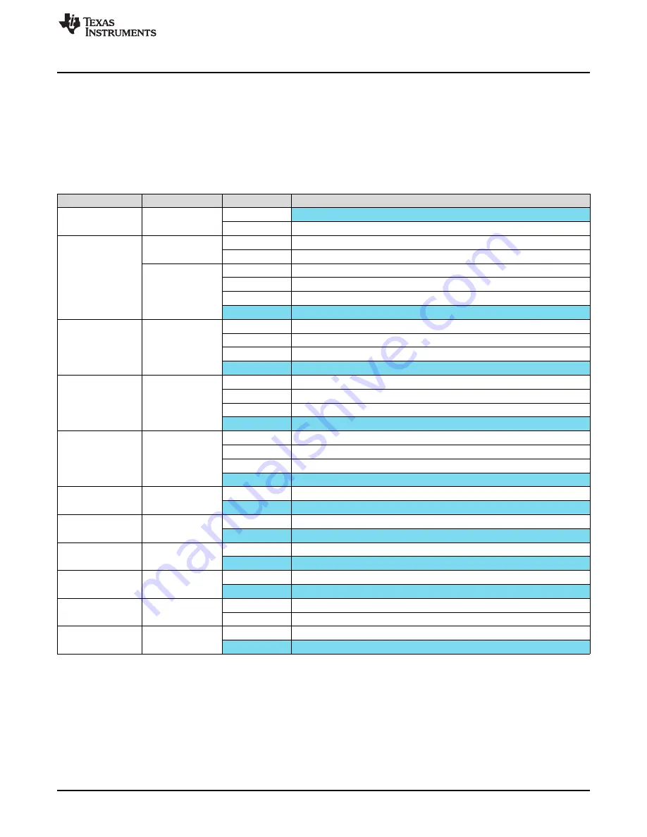
Table 19. Onboard Mux Settings and Control
MUX
Control Bits
Value
Mux Setting
A
n/a
n/a
QSPI Memory (default)
n/a
NOR Memory (Requires resistor change)
C (RU21)
SW5.3
OFF
NOR Memory
ON
EMMC Memory
EXP3.P[12:11]
00
Reserved
01
NOR Memory selected (by SW5.2)
10
EMMC Memory selected (by SW5.3)
11
NOR Memory selected (default)
B (RU88, RU94,
RU33)
EXP2.P[7,0]
00
Reserved
01
VIN1A to Expansion
10
VOUT3 to LCD Panel
11
GPMC NOR/NAND (default)
E (RU30)
EXP3.P[6,2]
00
Reserved
01
VIN2A to LI Camera
10
VIN2A to Expansion
11
Reserved (default)
F (RU93)
EXP3.P[12,11]
00
Reserved
01
VIN2A to LI Camera
10
VIN2A to Expansion
11
RGMII1 to Ethernet Port 1 (default)
K (RU111)
EXP2.P16
0
UART3 to COM8Q
1
Route to Expansion (SPI2) (default)
L (RU113)
EXP2.P3
0
Route to Expansion (I2C3)
1
Route to DCAN2 Connector (default)
J (RU95)
EXP2.P4
0
Route to Expansion (VIN1B)
1
RGMII0 to Ethernet Port 0 (default)
M (RU117)
EXP3.P13
0
Route to Expansion (VIN2B)
1
Route to Expansion (MMC3/legacy)(default)
G (RU96)
SW5.7
OFF
Use Default NOR Address (default)
ON
Use Alternate NOR Address (w/ EMMC)
H (RU99)
EXP3.P1
0
Route to COM8Q (MASP3/7)
1
Route to Expansion (McASP3/7)(default)