background image

1.3

System Requirements

1.4

Electrostatic Discharge Warning

1.5

Function Control for DAI Interface Format

1.6

Reset Operation

www.ti.com

System Requirements

The DEM-DSD1796/PCM1795/PCM1796/PCM1798 EVM has the following requirements:

• ±

15-V analog power supply at AVCC+, AVCC–, and GND

5-V DAC power supply at VCC and GND

S/PDIF input (sampling rate f

S

is up to 96 kHz) connected at the coaxial or optical connector

RCA analog output connected at CN103 (Lch) and CN104 (Rch); analog full-scale output level is 4.5
V

RMS

.

PC connected to printer connector CN003 for demonstration software operation (if necessary)

Appropriate test module:

DEM-PCM1795: for PCM1795

DEM-PCM1796: for PCM1796

DEM-DSD1796: for DSD1796

DEM-PCM1798: for PCM1798

Many of the components on the DEM-DSD1796/PCM1795/PCM1796/PCM1798 EVM are susceptible to
damage by electrostatic discharge (ESD). Customers are advised to observe proper ESD handling
precautions when unpacking and handling the EVM, including the use of a grounded wrist strap at an
approved ESD workstation.

CAUTION

Failure to observe ESD handling procedures may result in damage to EVM
components.

SW001, SW002, and SW003 are switches for controlling the audio interface format of the DAI receiver
CS8414. The default audio interface format of the DSD1796/PCM1795/PCM1796/PCM1798 is I

2

S™

format.

Table 1-1

lists the digital audio receiver configuration parameters.

Table 1-1. Digital Audio Receiver Configuration

Receiver Output Data

SW001

SW002

SW003

Format

L

L

L

16- to 24-bit left–justified

L

H

L

16- to 24-bit l2S

16-bit right-justified (or

H

L

H

standard)

18-bit right-justified (or

L

H

H

standard)

Pressing the SW004 pushbutton initiates a reset operation of the CS8414.

SLEU057A – September 2004 – Revised May 2009

Description

9

Submit Documentation Feedback

Summary of Contents for DEM-DSD1796

Page 1: ...DEM DSD1796 PCM1795 PCM1796 PCM1798 DSD1796 PCM1795 PCM1796 PCM1798 Evaluation Module User s Guide Literature Number SLEU057A September 2004 Revised May 2009...

Page 2: ...2 SLEU057A September 2004 Revised May 2009 Submit Documentation Feedback...

Page 3: ...ection 10 1 9 Demonstration Software 10 2 Schematics PCB Layout and Bill of Materials 11 2 1 DEM DAI ASDAC Printed Circuit Board Layout 12 2 2 DEM AS CDAC Printed Circuit Board Layout 15 2 3 DEM DAI A...

Page 4: ...CDAC Bottom View 16 2 7 DEM DAI ASDAC Analog Section Sockets for Daughterboard and Low Pass Filter 17 2 8 DEM DAI ASDAC Connector and Regulator 17 2 9 DEM DAI ASDAC Digital Section Digital Audio Inte...

Page 5: ...ion About Cautions and Warnings This document contains caution statements CAUTION This is an example of a caution statement A caution statement describes a situation that could potentially damage your...

Page 6: ...Trademarks www ti com Trademarks All trademarks are the property of their respective owners Read This First 6 SLEU057A September 2004 Revised May 2009 Submit Documentation Feedback...

Page 7: ...and circuitry for interfacing to audio test systems and commercial audio equipment Topic Page 1 1 Functional Block Diagram 8 1 2 EVM Features 8 1 3 System Requirements 9 1 4 Electrostatic Discharge Wa...

Page 8: ...alanced amplifier with a post low pass filter LPF section The DEM DSD1796 PCM1795 PCM1796 PCM1798 requires a 5 V digital power supply for its digital circuits a 5 V analog power supply for the device...

Page 9: ...EVM are susceptible to damage by electrostatic discharge ESD Customers are advised to observe proper ESD handling precautions when unpacking and handling the EVM including the use of a grounded wrist...

Page 10: ...monstration software is provided to control the PCM1796 DSD1796 internal register using a PC that is running the Microsoft Windows operating system This software uses a printer cable to connect the PC...

Page 11: ...e Board layouts are not to scale These are intended to show how the board is laid out they are not intended to be used for manufacturing DEM DAI1753 54 55 EVM PCBs Topic Page 2 1 DEM DAI ASDAC Printed...

Page 12: ...Board Layout www ti com Figure 2 1 through Figure 2 3 illustrate the printed circuit board PCB layout for the DEM DAI ASDAC Figure 2 1 DEM DAI ASDAC Silkscreen 12 Schematics PCB Layout and Bill of Mat...

Page 13: ...ti com DEM DAI ASDAC Printed Circuit Board Layout Figure 2 2 DEM DAI ASDAC Top View SLEU057A September 2004 Revised May 2009 Schematics PCB Layout and Bill of Materials 13 Submit Documentation Feedba...

Page 14: ...DAI ASDAC Printed Circuit Board Layout www ti com Figure 2 3 DEM DAI ASDAC Bottom View Schematics PCB Layout and Bill of Materials 14 SLEU057A September 2004 Revised May 2009 Submit Documentation Feed...

Page 15: ...rcuit Board Layout Figure 2 4 through Figure 2 6 illustrate the PCB layout for the DEM AS CDAC Figure 2 4 DEM AS CDAC Silkscreen Figure 2 5 DEM AS CDAC Top View SLEU057A September 2004 Revised May 200...

Page 16: ...M AS CDAC Printed Circuit Board Layout www ti com Figure 2 6 DEM AS CDAC Bottom View Schematics PCB Layout and Bill of Materials 16 SLEU057A September 2004 Revised May 2009 Submit Documentation Feedba...

Page 17: ...110 200 CN104 RCA pj 7 AVCC C110 10uF 16V C112 10uF 16V AVCC C108 8200pF R108 180 R104 220 R112 200 VDD C056 10uF 16V C054 100uF 16V C053 100uF 16V C051 0 1uF C052 100uF 16V 2 1 3 GND IN OUT C055 0 1u...

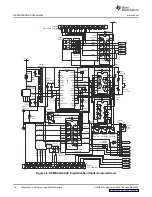
Page 18: ...BCK LRCK BCK INV INT CS8414 EXT DAI select LRCK BCK DATA SCLK LRCK BCK DATA SCLK BCK e DATA C014 GND U006 74VHC244 1 19 CN003 57LE 40360 7700 D3 SW006 DSS104 RA001 47k x5 ML MC MDI RST MDO RST MDO 1...

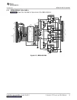
Page 19: ...C023 2700pF C026 10uF 16V C025 10uF 16V DSDL DSDR DBCK PLRCK WDCK PDATA DFD PDI PBCK SCKI DGND VDD MS MDI MC MDO RST C004 0 1uF C006 10uF 16V R002 10k C003 10uF 16V C001 10uF 16V U001 DSD1796 R001 C0...

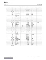
Page 20: ...8 R009 R010 mounted 1 U001 DAC 28 pin DSD1796 TIJ SSOP PCM1796 PCM1798 4 U002 U003 U004 Op amp 8 pin SOP NJM5534M JRC U005 Table 2 2 lists the bill of materials for the DEM DAI ASDAC_96 98 Table 2 2 B...

Page 21: ...JP001 4 pin connector FFC 4BMEP1 Yamaichi 1 R001 Resistor 75 SN14C2C 75 F KOA 1 R003 Resistor 47 k SN14C2C 47k F KOA 2 R002 R004 Resistor 470 SN14C2C 470 F KOA 4 R101 R104 Resistor 220 SN14C2C 220 F K...

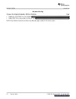
Page 22: ...on Page Updated document format to current standards 5 Added PCM1795 to devices relevant to this user guide 5 NOTE Page numbers for previous revisions may differ from page numbers in the current versi...

Page 23: ...the product This notice contains important safety information about temperatures and voltages For additional information on TI s environmental and or safety programs please contact the TI application...

Page 24: ...ce TI is not responsible or liable for any such statements TI products are not authorized for use in safety critical applications such as life support where a failure of the TI product would reasonabl...

Reviews: