Texas Instruments DAC8881 User Manual Download Page 4

DAC Module

VCC

VSS

VCC

GND

GND

VDD

(J6 )

(P 6 )

(J3 )

SCLK

W4

VSS

SDI

(J4)

(P4)

(W9)
(W3)

(W12)

CS

VSS

± 5 VA

+ 3 .3 VD

FS

U4A

TP2

TP8

W8

LDAC

RST

+ 1 .8 VD

+ 3 .3 VA

U4B

TP1

+ 5 VA

W11

W1

+ 3 .3 VA

VCC + 5 VA

U2

TP3

SDO

(J2 )

(P 2 )

(W 6 )

(W 10 )

W5

REF5050

OPA277

V

H

REF

V

L

REF

IOV

DD

V

L

REF

V

H

REF

AV

DD

DV

DD

IOV

DD

V

OUT

R

FB

DGND

AGND

PCB Design and Performance

www.ti.com

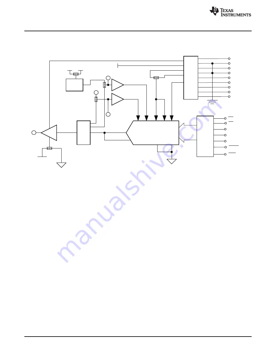
The DAC output can be monitored through pins 2 and 6 of the J4 header connector. The DAC output can
be switched through the W2 jumper for stacking the EVM for daisy-chaining purposes.

A block diagram of the EVM is shown in the

Figure 1

.

Figure 1. Block Diagram

2

PCB Design and Performance

This chapter describes the layout design of the PCB, the physical and mechanical characteristics of the
EVM, and the EVM test performance procedure performed. The list of components on this evaluation
module is also included in this section.

2.1

PCB Layout

The DAC8881 EVM is designed to preserve the performance quality of the DAC, device under test, as
specified in the datasheet. Carefully analyzing the physical restrictions of the EVM and the given or known
elements that contribute to performance degradation of the EVM is key to a successful design
implementation. These obvious attributes that diminish the performance of the EVM can be addressed
during the schematic design phase by selecting appropriate components and building a correct circuit. The
circuit should include adequate bypassing, identifying and managing analog and digital signals, and
knowing or understanding the mechanical attributes of the components.

The critical part of the design is the layout process. The main concern is primarily the placement of
components and the proper routing of signals. The bypass capacitors should be placed as close as
possible to the pins, and the analog and digital signals should be properly separated from each other. The
power and ground plane is very important and should be carefully considered in the layout process. A
solid plane is ideally preferred but sometimes impractical, so when a solid plane is not possible, a split
plane is an acceptable alternative. When considering a split plane design, analyze component placement
and carefully split the board into its analog and digital sections starting from the device under test. The
ground plane plays an important role in controlling noise and other effects that otherwise contribute to the
error of the DAC output. To ensure that the return currents are handled properly, route the appropriate
signals only in their respective sections, meaning the analog traces should only lay directly above or below
the analog section and the digital traces in the digital section. Minimize the length of the traces but use the
largest possible trace width allowable in the design. These design practices can be seen in the following
figures.

4

DAC8881 Evaluation Module

SLAU257A – September 2008 – Revised November 2009

Submit Documentation Feedback

Copyright © 2008–2009, Texas Instruments Incorporated

Summary of Contents for DAC8881

Page 1: ...Jumper Settings 14 3 6 Schematics 16 4 Using the DAC8881EVM with DXP 16 4 1 Hardware 17 4 2 MMB0 Power Supplies 17 4 3 Software Running DXP 18 4 4 DAC Output Update Options 20 4 5 Data Input Format 2...

Page 2: ...rint of U3 is compatible with many SO 8 package type reference devices so the user has the flexibility to select the reference supply to set the output range of the DAC8881 other than what is provided...

Page 3: ...ected Shorting pins 2 and 3 of both jumpers selects the reference voltages that are applied via J4 pins 18 and 20 respectively These voltages normally come from the host platform that is interfaced wi...

Page 4: ...should include adequate bypassing identifying and managing analog and digital signals and knowing or understanding the mechanical attributes of the components The critical part of the design is the la...

Page 5: ...s dimensions of 43 1800 mm 1 7000 inch 82 5500 mm 3 2500 inch and the board thickness is 1 5748 mm 0 062 inch Figure 2 through Figure 8 show the individual artwork layers Figure 2 Top Silkscreen Figur...

Page 6: ...www ti com Figure 4 Layer 2 Ground Plane Figure 5 Layer 3 Power Plane 6 DAC8881 Evaluation Module SLAU257A September 2008 Revised November 2009 Submit Documentation Feedback Copyright 2008 2009 Texas...

Page 7: ...rformance Figure 6 Layer 4 Bottom Signal Plane Figure 7 Bottom Silkscreen 7 SLAU257A September 2008 Revised November 2009 DAC8881 Evaluation Module Submit Documentation Feedback Copyright 2008 2009 Te...

Page 8: ...ware The EVM board is tested for all codes of 65535 and the device under test DUT is allowed to settle for 1ms before the meter is read This process is repeated for all codes to generate the measureme...

Page 9: ...6 10 F 1210 ceramic cap X7R 16V TDK C3225B63X7R1C106Z 4 7 C1 C2 C3 C4 C7 C15 C17 0 1 F 0805 ceramic cap X7R 50V 10 TDK C2012X7R1H104K 5 2 C9 C10 1 F 0805 ceramic cap X7R 16V 10 TDK C3216X7R1C105K 6 2...

Page 10: ...MMH 102 01 T T 28 10 Shunt 2mm shunt black Samtec 2SN BK G 29 0 R5 R7 R25 2 DNP 30 1 Shunt 0 100 shunt black Samtec SNT 100 BK T 1 P2 P4 and P6 parts are not shown in the schematic diagram All P desig...

Page 11: ...is connected to the noninverting input of the op amp U2 Figure 10 DAC8881 EVM Default Jumper Configuration 3 2 Host Processor Interface The host processor basically drives the DAC so the DACs proper...

Page 12: ...nd the signal used depends on the host controller that is selected to communicate with the DAC8881EVM Either signal can be chosen to drive the DAC8881 chip select CS pin The basic function of the CS a...

Page 13: ...the connector J4 The selected pins of the J4 connector as dictated by the jumper positions of the W2 and W7 jumpers can then be connected to the load to close the loop The EVM includes an external op...

Page 14: ...e loads Increasing the gain enhances the ability of the amplifier to drive even more capacitance and by adding a load resistor even improves the capacitive load drive capability Table 6 shows the jump...

Page 15: ...is is the default mode of the EVM from the factory Routes the reference feedback RFB pin of the DAC8881 to J4 pin 8 to provide the option to close the output op amp U2 loop as close as possible to the...

Page 16: ...wn status If jumper is installed on pins 13 and 14 the SDOSEL pin of the DAC8881 is tied to ground so that the DAC device can be operated in daisy chain mode DAC8881 IOVDD is powered with 5VD J3 DAC88...

Page 17: ...3 100 W12 W3 R1 0 CS VOUT1 VOUT2 TP5 IOVDD RFB RFB1 RFB2 W2 W7 Do not populate R5 R7 R25 W8 3 2 6 7 4 8 U5 OPA277 1 First Proto Release JLP J PARGUIAN 6489897 1 AVDD 5 VREFH 11 RFB 9 VOUT 8 CS 19 SCLK...

Page 18: ...O NOT connect the MMB0 to your PC before installing the DXP software as described in the DXP User s Guide Installing the software will ensure the necessary drivers are properly loaded to run the hardw...

Page 19: ...MMB0 Connect all other analog supplies as necessary to J14 on the MMB0 4 3 Software Running DXP Install DXP on a laptop or personal computer running Windows XP as per the detailed instruction in the...

Page 20: ...lease ensure no jumpers are placed on J1 pins 9 10 When the RST pin is low the device is in hardware reset mode and the input register and DAC latch are set to the value defined by the RSTSEL pin refe...

Page 21: ...1 2 routes the LDAC input to pin 15 of J2 This feature allows the user to Timer apply an LDAC input from an external source In this mode J2 pin 15 provides an interrupt to the DSP on the MMB0 which tr...

Page 22: ...terature Number DAC8881 SBAS422 REF02 SBVS003 REF5050 SBOS410 REF5045 SBOS410 OPA211 SBVS058 OPA627 SBOS165 OPA277 SBOS079 OPA2277 SBOS079 OPA227 SBOS110 5 2 Questions About This or Other Data Convert...

Page 23: ...oduct This notice contains important safety information about temperatures and voltages For additional information on TI s environmental and or safety programs please contact the TI application engine...

Page 24: ...ce TI is not responsible or liable for any such statements TI products are not authorized for use in safety critical applications such as life support where a failure of the TI product would reasonabl...

Page 25: ...Mouser Electronics Authorized Distributor Click to View Pricing Inventory Delivery Lifecycle Information Texas Instruments DAC8881EVM...

Reviews: