RXENA
RXRDY
1
6
3
4
5
2
0
1
2
3
4
5
0
1
2
Start
Stop
Start
Ad
Pa
SCIRXD pin
Frame
Majority
vote
Start bit
LSB of data
SC ICLK
(internal)
SCIRXD
1
2
3
4
5
6
7
8
1
2
3
4
5
6
7
8
1
8 SCICLK periods per data bit
8 SCICLK periods per data bit
Enhanced SCI Module Overview
988
SPRUH22I – April 2012 – Revised November 2019
Copyright © 2012–2019, Texas Instruments Incorporated
C28 Serial Communications Interface (SCI)
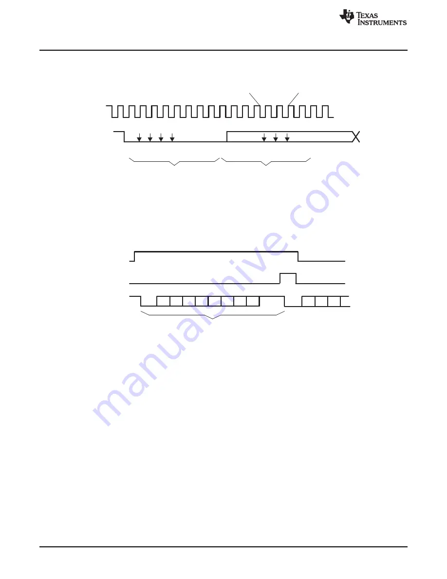
Since the receiver synchronizes itself to frames, the external transmitting and receiving devices do not
have to use a synchronized serial clock. The clock can be generated locally.
Figure 13-7. SCI Asynchronous Communications Format
13.1.1.7.1 Receiver Signals in Communication Modes
illustrates an example of receiver signal timing that assumes the following conditions:
•
Address-bit wake-up mode (address bit does not appear in idle-line mode)
•
Six bits per character
Figure 13-8. SCI RX Signals in Communication Modes
(1)
Data arrives on the SCIRXD pin, start bit detected.
(2)
Bit RXENA is brought low to disable the receiver. Data continues to be assembled in RXSHF but is not
transferred to the receiver buffer register.
Notes:
1. Flag bit RXENA (SCICTL1, bit 0) goes high to enable the receiver.
2. Data arrives on the SCIRXD pin, start bit detected.
3. Data is shifted from RXSHF to the receiver buffer register (SCIRXBUF); an interrupt is requested. Flag
bit RXRDY (SCIRXST, bit 6) goes high to signal that a new character has been received.
4. The program reads SCIRXBUF; flag RXRDY is automatically cleared.
5. The next byte of data arrives on the SCIRXD pin; the start bit is detected, then cleared.
6. Bit RXENA is brought low to disable the receiver. Data continues to be assembled in RXSHF but is not
transferred to the receiver buffer register.
13.1.1.7.2 Transmitter Signals in Communication Modes
illustrates an example of transmitter signal timing that assumes the following conditions:
•
Address-bit wake-up mode (address bit does not appear in idle-line mode)
•
Three bits per character


