TOUT1
CPU TIMER2
CPU TIMER0
Watchdog
Peripherals
TINT0
XINT1
Interrupt Control
XINT1
XINT1 CR (15:0)
Interrupt Control
XINT2
XINT2CR(15:0)
GPIO
Mux
WDINT
NMI
XINT1 CTR (15:0)
XINT2CTR(15:0)
CPU TIMER1
TINT2
Low Power Modes
LPMINT
WAKEINT
TINT1
Sync
SYSCLKOUT
Flash Wrapper
XINT2
XINT3
GPTRIP4SEL(5:0)
GPTRIPSEL(5:0)
GPTRIPSEL(5:0)
Interrupt Control
XINT3
XINT3CR(15:0)
XINT3CTR(15:0)
NMI Interrupt With Watchdog Function
NMIRS
System Control
INT14
GPIO0 .int
GPIO63. int
CPUTMR2CLK
M
U
X
M
U
X
P
I
E
U
p
T
o
9
6
I
n
t
e
r
r
u
p
t
s
M
U
X
INT13
C28
Core
INT1
INT12
to
Exceptions and Interrupts Control
106
SPRUH22I – April 2012 – Revised November 2019
Copyright © 2012–2019, Texas Instruments Incorporated
System Control and Interrupts
1.5.4.3
Interrupt Sources
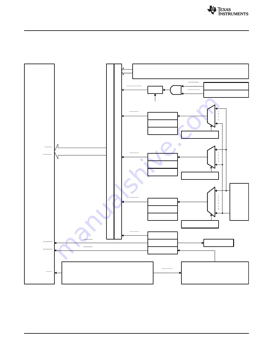
shows how the various interrupt sources are multiplexed within the devices. This multiplexing
(MUX) scheme may not be exactly the same on all 28x devices. See the device data manual for details.
Figure 1-7. PIE Interrupt Sources and External Interrupts XINT1/XINT2/XINT3
1.5.4.3.1 Procedure for Handling Multiplexed Interrupts
The PIE module multiplexes eight peripheral and external pin interrupts into one CPU interrupt. These
interrupts are divided into 12 groups: PIE group 1 - PIE group 12. Each group has an associated enable
PIEIER and flag PIEIFR register. These registers are used to control the flow of interrupts to the CPU. The
PIE module also uses the PIEIER and PIEIFR registers to decode to which interrupt service routine the
CPU should branch.


