background image

8 Specifications

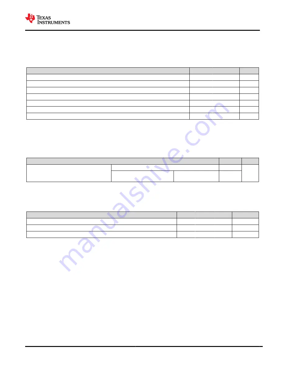
8.1 Absolute Maximum Ratings

All measurements are referenced at the module pins unless otherwise indicated. All specifications are over process and 
voltage unless otherwise indicated.
Over operating free-air temperature range (unless otherwise noted)

(1)


(2)

MIN

MAX

UNIT

V

BAT

–0.5

3.8

V

Digital I/O

–0.5

V

BAT

 + 0.5

V

RF pin

–0.5

2.1

V

Analog pins

–0.5

2.1

V

Operating temperature (T

A

)

–40

85

°C

Storage temperature (T

stg

)

–40

85

°C

Junction temperature (T

j

)

(3)

120

°C

(1)

Stresses beyond those listed under 

Absolute Maximum Ratings

 may cause permanent damage to the device. These are stress ratings 

only, and functional operation of the device at these or any other conditions beyond those indicated under 

Recommended Operating 

Conditions

 is not implied. Exposure to absolute-maximum-rated conditions for extended periods may affect device reliability.

(2)

All voltage values are with respect to V

SS

, unless otherwise noted.

(3)

Junction temperature is for the CC3220x device that is contained within the module.

8.2 ESD Ratings

VALUE

UNIT

V

ESD

Electrostatic discharge

Human body model (HBM), per ANSI/ESDA/JEDEC JS001

(1)

±2000

V

Charged device model (CDM),
per JESD22-C101

(2)

All pins

±500

(1)

JEDEC document JEP155 states that 500-V HBM allows safe manufacturing with a standard ESD control process.

(2)

JEDEC document JEP157 states that 250-V CDM allows safe manufacturing with a standard ESD control process.

8.3 Recommended Operating Conditions

over operating free-air temperature range (unless otherwise noted)

(2)


(1)(3)

MIN

TYP

MAX

UNIT

V

BAT

2.3

3.3

3.6

V

Operating temperature

–40

25

85

°C

Ambient thermal slew

–20

20

°C/minute

(1)

When operating at an ambient temperature of over 75°C, the transmit duty cycle must remain below 50% to avoid the auto-protect 
feature of the power amplifier. If the auto-protect feature triggers, the device takes a maximum of 60 seconds to restart the 
transmission.

(2)

To ensure WLAN performance, the ripple on the power supply must be less than ±300 mV. The ripple should not cause the supply to 
fall below the brownout voltage.

(3)

The minimum voltage specified includes the ripple on the supply voltage and all other transient dips. The brownout condition is also 2.1 
V, and care must be taken when operating at the minimum specified voltage.

www.ti.com

CC3220MOD, CC3220MODA

SWRS206E – MARCH 2017 – REVISED MAY 2021

Copyright © 2021 Texas Instruments Incorporated

Submit Document Feedback

27

Product Folder Links: 

CC3220MOD


CC3220MODA

Summary of Contents for CC3120MOD

Page 1: ...faces JTAG cJTAG and SWD Wi Fi network processor subsystem Wi Fi Internet on a chip dedicated Arm MCU completely offloads Wi Fi and internet protocols from the application MCU Wi Fi Modes 802 11b g n Station 802 11b g n Access Point Supports up to Four Stations Wi Fi Direct Client and Group Owner WPA2 Personal and Enterprise Security WEP WPA WPA2 PSK and WPA2 Enterprise 802 1x WPA3 personal and en...

Page 2: ... mA measured on CC3220MODS CC3220MODSF and CC3220MODASF consume an additional 15 mA at 54 OFDM maximum power Idle connected MCU in LPDS 710 µA measured on CC3220MODS and CC3220MODSF with 256KB RAM retention at DTIM 1 Additional integrated components 40 0 MHz crystal 32 768 kHz crystal RTC 32 Mbit SPI Serial Flash RF filter and passive components Footprint compatible QFM package CC3220MODx 1 27 mm ...

Page 3: ...s low power consumption modes for extended battery life such as low power deep sleep hibernate with RTC consuming only 5 µA and shutdown mode consuming only 1 µA The module includes a wide variety of peripherals including a fast parallel camera interface I2S SD UART SPI I2C and a 4 channel ADC The SimpleLink CC3220MODx and CC3220MODAx module family come in four different module variants CC3220MODS...

Page 4: ...DY SIZE NOM CC3220MODSM2MOBR QFM 63 20 50 mm 17 50 mm CC3220MODSF12MOBR QFM 63 20 50 mm 17 50 mm CC3220MODASM2MONR QFM 63 25 50 mm 20 50 mm CC3220MODASF12MONR QFM 63 25 50 mm 20 50 mm 1 For more information see Section 13 CC3220MOD CC3220MODA SWRS206E MARCH 2017 REVISED MAY 2021 www ti com 4 Submit Document Feedback Copyright 2021 Texas Instruments Incorporated Product Folder Links CC3220MOD CC322...

Page 5: ...er GPIOs 32 Mbit SFlash External SPI Programming 40 MHz 32 768 kHz UART SPI nReset PM 2 3 V to 3 6 V VBAT Figure 4 1 CC3220MODx Functional Block Diagram www ti com CC3220MOD CC3220MODA SWRS206E MARCH 2017 REVISED MAY 2021 Copyright 2021 Texas Instruments Incorporated Submit Document Feedback 5 Product Folder Links CC3220MOD CC3220MODA ...

Page 6: ...corporated Figure 4 2 CC3220MODAx Functional Block Diagram For 3200MOD module pin multiplexing details see the CC3200 SimpleLink Wi Fi Wireless and Internet of Things Solution a Single Chip Wireless MCU data sheet Figure 4 3 CC3200MOD Module Functional Block Diagram CC3220MOD CC3220MODA SWRS206E MARCH 2017 REVISED MAY 2021 www ti com 6 Submit Document Feedback Copyright 2021 Texas Instruments Inco...

Page 7: ...io Synthesizer Copyright 2017 Texas Instruments Incorporated Figure 4 4 CC3220x Hardware Overview Figure 4 5 shows the an overview of the CC3220x embedded software Customer Application Peripherals Driver SimpleLink Driver APIs NetApp BSD Socket Wi Fi Host Interface Network Applications WLAN Security and Management TCP IP Stack WLAN MAC and PHY Applications MCU Network Processor Figure 4 5 CC3220x ...

Page 8: ...Qualification 58 9 11 Module Markings 60 9 12 End Product Labeling 62 9 13 Manual Information to the End User 62 10 Applications Implementation and Layout 63 10 1 Typical Application 64 10 2 Device Connection and Layout Fundamentals 67 10 3 PCB Layout Guidelines 67 11 Environmental Requirements and Specifications 73 11 1 PCB Bending 73 11 2 Handling Environment 73 11 3 Storage Condition 73 11 4 Ba...

Page 9: ...er Wireless Microcontroller Wireless Microcontroller Wireless Microcontroller Standard 802 11 b g n 802 11 b g n 802 11 b g n 802 11 b g n 802 11 b g n Frequency 2 4 GHz 2 4 GHz 2 4 GHz 2 4 GHz 2 4 GHz TCP IP Stack IPv4 IPv6 IPv4 IPv6 IPv4 IPv6 IPv4 IPv6 IPv4 IPv6 Sockets 16 16 16 16 16 Integrated MCU Arm Cortex M4 at 80 MHz Arm Cortex M4 at 80 MHz Arm Cortex M4 at 80 MHz Arm Cortex M4 at 80 MHz O...

Page 10: ... software and tool options for customers developing wired and wireless applications With 100 percent code reuse across host MCUs Wi Fi Bluetooth low energy Sub 1GHz devices and more choose the MCU or connectivity standard that fits your design A one time investment with the SimpleLink software development kit SDK allows you to reuse often opening the door to create unlimited applications Companion...

Page 11: ...L1 SOP1 SOP2 JTAG_TMS JTAG_TCK NC GPIO28 JTAG_TDO 32 33 34 35 36 37 38 39 40 41 42 43 31 29 28 30 45 48 49 50 44 46 47 51 52 53 54 GPIO0 NC GPIO1 GPIO2 GPIO3 GPIO4 GPIO5 GPIO6 GPIO7 GPIO8 GPIO9 GND NC GND RF_BG GND NC SOP0 nRESET VBAT_RESET VBAT1 GND NC VBAT2 NC GPIO30 GND CC3220MODx Pin Diagram Bottom View shows the approximate location of pins on the module For the actual mechanical diagram see ...

Page 12: ...EL2 ANT_SEL1 SOP1 SOP2 JTAG_TMS JTAG_TCK NC GPIO28 JTAG_TDO 32 33 34 35 36 37 38 39 40 41 42 43 31 29 28 30 45 48 49 50 44 46 47 51 52 53 54 GPIO0 NC GPIO1 GPIO2 GPIO3 GPIO4 GPIO5 GPIO6 GPIO7 GPIO8 GPIO9 GND NC GND RF_BG GND NC SOP0 nRESET VBAT_RESET VBAT1 GND NC VBAT2 NC GPIO30 GND PCB Antenna Figure 7 2 CC3220MODAx Pin Diagram Bottom View CC3220MOD CC3220MODA SWRS206E MARCH 2017 REVISED MAY 2021...

Page 13: ...connected if not used on product 2 23 SOP2 21 See Section 9 9 1 for SOP 2 0 configuration modes 24 SOP1 34 See Section 9 9 1 for SOP 2 0 configuration modes 25 ANT_SEL1 I O 29 Antenna selection control 2 26 ANT_SEL2 I O 30 Antenna selection control 2 27 GND Ground 28 GND Ground 30 GND Ground 31 RF_BG I O 31 2 4 GHz RF input output 32 GND Ground 34 SOP0 35 See Section 9 9 1 for SOP 2 0 configuratio...

Page 14: ...61 GND Thermal ground 62 GND Thermal ground 63 GND Thermal ground 1 I input O output I O bidirectional 2 For pin multiplexing details see Table 7 3 7 3 Connections for Unused Pins All unused pins must be left as no connect NC pins Table 7 1 and Table 7 2 list the NC pins on the CC3220MODx and CC3220MODAx modules respectively Table 7 1 Connections for Unused Pins PIN DEFAULT FUNCTION STATE AT RESET...

Page 15: ...ver the default state can be changed by SW All digital I Os are non fail safe Note If an external device drives a positive voltage to the signal pads and the CC3220MODx or CC3220MODAx modules are not powered DC is drawn from the other device If the drive strength of the external device is adequate an unintentional wakeup and boot of the CC3220MODx or CC3220MODAx modules can occur To prevent curren...

Page 16: ... data O 1 6 SDCARD_CL K SD card clock O 0 12 GT_CCP01 Timer capture port I Hi Z Pull Drive 4 GPIO11 I O Yes No No GPIO_PA D_ CONFIG_1 1 0x4402 E0CC 0 GPIO11 GPIO I O Hi Z Pull Drive Hi Z Pull Drive Hi Z 1 I2C_SDA I2C data I O open drain Hi Z Pull Drive 3 GT_PWM07 Pulse width modulated O P O Hi Z Pull Drive 4 pXCLK XVCLK Free clock to parallel camera O 0 6 SDCARD_C MD SD card command line I O open ...

Page 17: ...ONFIG_1 5 0x4402 E0DC 0 GPIO15 GPIO I O Hi Z Pull Drive Hi Z Pull Drive Hi Z 5 I2C_SDA I2C data I O open drain 7 GSPI_MISO General SPI MISO I O 4 pDATA9 CAM_D5 Parallel camera data bit 5 I 13 GT_CCP06 Timer capture port I 8 SDCARD_ DATA0 SD card data I O 7 GPIO16 I O No No No GPIO_PA D_ CONFIG_1 6 0x4402 E0E0 0 GPIO16 GPIO I O Hi Z Pull Drive Hi Z Pull Drive Hi Z Hi Z Pull Drive Hi Z Pull Drive 7 ...

Page 18: ...l Drive Hi Z 3 McACLK I2S audio port clock output O Hi Z Pull Drive 4 pVS VSYNC Parallel camera vertical sync I Hi Z Pull Drive 5 I2C_SCL I2C clock I O open drain Hi Z Pull Drive 7 UART0_TX UART0 TX data O 1 12 GT_CCP03 Timer capture port I Hi Z Pull Drive 10 GPIO13 I O Yes No No GPIO_PA D_ CONFIG_1 3 0x4402 E0D4 0 GPIO13 GPIO I O Hi Z Pull Drive Hi Z Pull Drive Hi Z 5 I2C_SDA I2C data I O open dr...

Page 19: ... N A N A N A N A N A FLASH_SPI_ CLK Clock to SPI serial Flash fixed default N A Hi Z Pull Drive 3 Hi Z Pull Drive Hi Z 16 GND GND N A N A N A N A N A GND GND N A N A N A N A 17 FLASH_ SPI_ MOSI N A N A N A N A N A N A FLASH_SPI_ MOSI Data to SPI serial Flash fixed default N A Hi Z Pull Drive 3 Hi Z Pull Drive Hi Z 18 JTAG_T DO I O Yes No Muxed with JTAG TDO GPIO_PA D_ CONFIG_ 24 0x4402 E100 1 TDO ...

Page 20: ...th modulated O P O Hi Z Pull Drive 2 McAFSX I2S audio port frame sync O Hi Z Pull Drive See 5 TCXO_EN Enable to optional external 40 MHz TCXO O 0 See 6 SOP2 Sense on power 2 I Hi Z Pull Drive 24 SOP1 Config sense N A N A N A N A N A SOP1 Sense on power 1 N A N A N A N A 25 7 ANT_SE L1 O only No User config not requir ed 8 No GPIO_PA D_ CONFIG_2 6 0x4402 E108 0 ANTSEL1 3 Antenna selection control O...

Page 21: ...37 VBAT1 Supply input N A N A N A N A N A VBAT1 Analog DC DC input connected to chip input supply VBAT N A N A N A N A 38 GND GND N A N A N A N A N A GND GND N A N A N A N A 39 NC WLAN analog N A N A N A N A N A NC Reserved N A N A N A N A 40 VBAT2 Supply input N A N A N A N A N A VBAT2 Analog input supply VBAT N A N A N A N A 41 NC WLAN analog N A N A N A N A N A NC Reserved N A N A N A N A 42 GP...

Page 22: ...7 GT_CCP00 Timer capture port I Hi Z Pull Drive 9 GSPI_CS General SPI chip select I O Hi Z Pull Drive 10 UART1_RTS UART1 Request to Send active low O 1 3 UART0_RTS UART0 Request to Send active low O 1 4 McAXR0 I2S audio port data 0 RX TX I O Hi Z Pull Drive 45 NC WLAN analog N A N A N A N A N A NC Reserved N A N A N A N A 46 GPIO1 I O No No No GPIO_PA D_ CONFIG_1 0x4402 E0A4 0 GPIO1 GPIO I O Hi Z ...

Page 23: ...capture port I Hi Z Pull Drive 48 10 GPIO3 Analog input up to 1 8 V digital I O No See 9 No GPIO_PA D_ CONFIG_3 0x4402 E0AC See 5 ADC_CH1 ADC channel 1 input 1 5 V max I Hi Z Pull Drive Hi Z Pull Drive Hi Z 0 GPIO3 GPIO I O Hi Z Pull Drive 6 UART1_TX UART1 TX data O 1 4 pDATA7 CAM_D3 Parallel camera data bit 3 I Hi Z Pull Drive 49 10 GPIO4 Analog input up to 1 8 V digital I O Yes See 9 Yes GPIO_PA...

Page 24: ...ull Drive 51 GPIO6 I O No No No GPIO_PA D_ CONFIG_6 0x4402 E0B8 0 GPIO6 GPIO I O Hi Z Pull Drive Hi Z Pull Drive Hi Z 5 UART0_RTS UART0 Request to Send active low O 1 4 pDATA4 CAM_D0 Parallel camera data bit 0 I Hi Z Pull Drive 3 UART1_CTS UART1 Clear to send active low I Hi Z Pull Drive 6 UART0_CTS UART0 Clear to send active low I Hi Z Pull Drive 7 GT_CCP06 Timer capture port I Hi Z Pull Drive 52...

Page 25: ...Pull Drive Hi Z 3 GT_PWM05 Pulse width modulated O P O 6 SDCARD_ DATA0 SD card data I O 7 McAXR0 I2S audio port data RX TX I O 12 GT_CCP00 Timer capture port I 55 GND GND N A N A N A N A N A GND GND N A N A N A N A 56 GND GND N A N A N A N A N A GND GND N A N A N A N A 57 GND GND N A N A N A N A N A GND GND N A N A N A N A 58 GND GND N A N A N A N A N A GND GND N A N A N A N A 59 GND GND N A N A N...

Page 26: ... state as are other digital I Os 4 48 Analog signal 1 8 V absolute 1 46 V full scale ADC is isolated The digital I O cell is also isolated Determined by the I O state as are other digital I Os 4 49 Analog signal 1 8 V absolute 1 46 V full scale ADC is isolated The digital I O cell is also isolated Determined by the I O state as are other digital I Os 4 50 Analog signal 1 8 V absolute 1 46 V full s...

Page 27: ... Charged device model CDM per JESD22 C101 2 All pins 500 1 JEDEC document JEP155 states that 500 V HBM allows safe manufacturing with a standard ESD control process 2 JEDEC document JEP157 states that 250 V CDM allows safe manufacturing with a standard ESD control process 8 3 Recommended Operating Conditions over operating free air temperature range unless otherwise noted 2 1 3 MIN TYP MAX UNIT VB...

Page 28: ... 8 1 Figure 8 2 and Figure 8 3 TX power level 4 implies output power backed off approximately 4 dB 2 CC3220MODx and CC3220MODAx are constant power source systems The active current numbers scale based on the VBAT voltage supplied 3 DTIM 1 4 The LPDS number of reported is with retention of 256KB of MCU SRAM The CC3220MODx and CC3220MODAx modules can be configured to retain 0KB 64KB 128KB 192KB or 2...

Page 29: ...M 53 NWP LPDS 5 135 µA NWP idle connected 4 710 µA MCU hibernate NWP hibernate 5 µA MCU shutdown NWP shutdown 1 Peak calibration current 5 VBAT 3 6 V 420 mA VBAT 3 3 V 450 VBAT 2 3 V 620 1 TX power level 0 implies maximum power see Figure 8 1 Figure 8 2 and Figure 8 3 TX power level 4 implies output power backed off approximately 4 dB 2 CC3220MODx and CC3220MODAx are constant power source systems ...

Page 30: ...current TX power level setting TX Power dBm 19 00 17 00 15 00 13 00 11 00 9 00 7 00 5 00 3 00 1 00 0 1 2 3 4 5 6 7 8 9 10 11 12 13 14 15 280 00 264 40 249 00 233 30 218 00 202 00 186 70 171 00 155 60 140 00 1 DSSS IBAT VBAT 3 6 V mAmp Color by TX Power dBm IBAT VBAT 3 6 V Figure 8 1 TX Power and IBAT vs TX Power Level Settings 1 DSSS TX power level setting TX Power dBm 19 00 17 00 15 00 13 00 11 0...

Page 31: ...0 233 30 218 00 202 00 186 70 171 00 155 60 140 00 IBAT VBAT 3 6 V mAmp Color by TX Power dBm IBAT VBAT 3 6 V Figure 8 3 TX Power and IBAT vs TX Power Level Settings 54 OFDM www ti com CC3220MOD CC3220MODA SWRS206E MARCH 2017 REVISED MAY 2021 Copyright 2021 Texas Instruments Incorporated Submit Document Feedback 31 Product Folder Links CC3220MOD CC3220MODA ...

Page 32: ... the wiring and PCB routing resistance Note When the module is in HIBERNATE state brownout is not detected Only blackout is in effect during HIBERNATE state Figure 8 4 Brownout and Blackout Levels 1 of 2 Figure 8 5 Brownout and Blackout Levels 2 of 2 In the brownout condition all sections of the device shut down within the module except for the Hibernate block including the 32 kHz RTC clock which ...

Page 33: ...O drive strength 4 mA 2 4 V VDD 3 6 V VDD 0 7 IL 6 mA configured I O drive strength 6 mA 2 4 V VDD 3 6 V VDD 0 7 IL 2 mA configured I O drive strength 2 mA 2 3 V VDD 2 4 V VDD 0 75 VOL Low level output voltage IL 2 mA configured I O drive strength 2 mA 2 4 V VDD 3 6 V VDD 0 2 V IL 4 mA configured I O drive strength 4 mA 2 4 V VDD 3 6 V VDD 0 2 IL 6 mA configured I O drive strength 6 mA 2 4 V VDD 3...

Page 34: ...nfigured I O drive strength 6 mA 2 4 V VDD 3 6 V VDD 0 2 IL 2 mA configured I O drive strength 2 mA 2 3 V VDD 2 4 V VDD 0 25 IOH High level source current VOH 2 4 2 mA drive 1 5 mA 4 mA drive 2 5 6 mA drive 3 5 IOL Low level sink current 2 mA drive 1 5 mA 4 mA drive 2 5 6 mA drive 3 5 VIL nRESET 2 0 6 V Pin Internal Pullup and Pulldown 25 C IOH Pullup current VDD 3 0 V 5 10 µA IOL Pulldown current...

Page 35: ...hannel 6 2437 MHz 1 2 PARAMETER RATE MIN TYP MAX UNIT Max RMS Output Power measured at 1 dB from IEEE spectral mask or EVM 1 DSSS 17 0 dBm 2 DSSS 17 0 11 CCK 17 3 6 OFDM 16 3 9 OFDM 16 3 18 OFDM 16 36 OFDM 15 54 OFDM 13 5 MCS7 mixed mode 12 Transmit center frequency accuracy 20 20 ppm 1 The edge channels 2412 MHz and 2462 MHz have reduced TX power to meet FCC emission limits 2 Power of 802 11b rat...

Page 36: ...rmal Conductivity Test Board for Leaded Surface Mount Packages JESD51 9 Test Boards for Area Array Surface Mount Package Thermal Measurements Power dissipation of 2 W and an ambient temperature of 70 C is assumed 3 m s meters per second 8 14 Timing and Switching Characteristics 8 14 1 Power Up Sequencing For proper start up of the CC3220MODx and CC3220MODAx modules perform the recommended power up...

Page 37: ...is properly applied A negative reset pulse on pin 35 of at least 200 mS duration 8 14 4 Wake Up From Hibernate Timing Table 8 3 lists the software hibernate timing requirements Note The internal 32 768 kHz crystal is kept enabled by default when the module goes to hibernate Table 8 3 Software Hibernate Timing Requirements ITEM NAME DESCRIPTION MIN TYP MAX UNIT THIB_MIN Minimum hibernate time 10 ms...

Page 38: ...ra parallel port External Flash UART SD Host Timers 8 14 5 1 SPI 8 14 5 1 1 SPI Master The CC3220MODx and CC3220MODAx microcontroller includes one SPI module which can be configured as a master or slave device The SPI includes a serial clock with programmable frequency polarity and phase a programmable timing control between chip select and external clock generation and a programmable delay before...

Page 39: ...ycle 45 55 T6 tIS 1 RX data setup time 1 ns T7 tIH 1 RX data hold time 2 ns T8 tOD 1 TX data output delay 8 5 ns T9 tOH 1 TX data hold time 8 ns 1 Timing parameter assumes a maximum load of 20 pF 8 14 5 1 2 SPI Slave Figure 8 9 shows the timing diagram for the SPI slave T2 T6 T7 T9 CLK MISO MOSI T8 Figure 8 9 SPI Slave Timing Diagram www ti com CC3220MOD CC3220MODA SWRS206E MARCH 2017 REVISED MAY ...

Page 40: ...e sync polarity A fractional divider is available for bit clock generation 8 14 5 2 1 I2S Transmit Mode Figure 8 10 shows the timing diagram for the I2S transmit mode T2 T1 T3 T4 McACLKX McAFSX McAXR0 1 T4 Figure 8 10 I2S Transmit Mode Timing Diagram Table 8 6 lists the timing parameters for the I2S transmit mode Table 8 6 I2S Transmit Mode Timing Parameters ITEM NAME DESCRIPTION MIN MAX UNIT T1 f...

Page 41: ...ldown strength weak 10 µA configurable drive strength 2 4 and 6 mA and open drain enable Figure 8 12 shows the GPIO timing diagram SWAS031 067 VDD 80 20 tGPIOF tGPIOR Figure 8 12 GPIO Timing Diagram Table 8 8 lists the GPIO output transition times for VBAT 2 3 V Table 8 8 GPIO Output Transition Times VBAT 2 3 V 1 2 DRIVE STRENGTH mA DRIVE STRENGTH CONTROL BITS Tr Tf UNIT MIN NOM MAX MIN NOM MAX 2 ...

Page 42: ...5 50 52 and 53 8 14 5 3 1 GPIO Input Transition Time Parameters Table 8 10 lists the input transition time parameters Table 8 10 GPIO Input Transition Time Parameters MIN MAX UNIT tr Input transition time tr tf 10 to 90 1 3 ns tf 1 3 ns 8 14 5 4 I2C The CC3220MODx and CC3220MODAx MCUs include one I2C module operating with standard 100 kbps or fast 400 kbps transmission speeds Figure 8 13 shows the...

Page 43: ...lue of the external signal capacitance and external pullup register 3 All timing is with 6 mA drive and 20 pF load 8 14 5 5 IEEE 1149 1 JTAG The Joint Test Action Group JTAG port is an IEEE standard that defines a test access port TAP and boundary scan architecture for digital integrated circuits and provides a standardized serial interface to control the associated test logic For detailed informa...

Page 44: ...ycles Sampling 4 cycles SAR Conversion 16 cycles Sampling 4 cycles SAR Conversion 16 cycles EXT CHANNEL 0 INTERNAL CHANNEL EXT CHANNEL 1 INTERNAL CHANNEL Internal Ch Figure 8 15 ADC Clock Timing Diagram Figure 8 15 shows the ADC clock timing diagram Table 8 13 ADC Electrical Specifications PARAMETER DESCRIPTION TEST CONDITIONS ASSUMPTIONS MIN TYP MAX UNIT Nbits Number of bits 12 Bits INL Integral ...

Page 45: ...external image sensors stores the image data in a FIFO and generates DMA requests The camera parallel port supports 8 bits Figure 8 16 shows the timing diagram for the camera parallel port pCLK pVS pHS pDATA T3 T2 T4 T6 T7 Figure 8 16 Camera Parallel Port Timing Diagram Table 8 14 lists the timing parameters for the camera parallel port Table 8 14 Camera Parallel Port Timing Parameters ITEM NAME D...

Page 46: ...th minimal LH intervention The SD host does the following Provides SD card access in 1 bit mode Deals with SD protocol at the transmission level Handles data packing Adds cyclic redundancy checks CRC Start and end bit Checks for syntactical correctness The application interface sends every SD command and either polls for the status of the adapter or waits for an interrupt request The result is the...

Page 47: ...fers The GPTM contains four 16 or 32 bit GPTM blocks with the following functional options Operating modes 16 or 32 bit programmable one shot timer 16 or 32 bit programmable periodic timer 16 bit general purpose timer with an 8 bit prescaler 16 bit input edge count or time capture modes with an 8 bit prescaler 16 bit PWM mode with an 8 bit prescaler and software programmable output inversion of th...

Page 48: ...d of state saving and restoration between interrupts Processor state automatically saved on interrupt entry and restored on interrupt exit with no instruction overhead Wake up interrupt controller WIC providing ultra low power sleep mode support Bus interfaces Advanced high performance bus AHB Lite interfaces system bus interfaces Bit band support for memory and select peripheral that includes ato...

Page 49: ...ilities of the host MCU thus it is usable by deeply embedded applications 802 11 transceiver mode allows transmitting and receiving of proprietary data through a socket without adding MAC or PHY headers The 802 11 transceiver mode provides the option to select the working channel rate and transmitted power The receiver mode works with the filtering options 9 3 2 Network Stack The Network Stack fea...

Page 50: ... Network applications and utilities Ping HTTP HTTPS web server mDNS DNS SD DHCP server Host interface UART SPI Security Device identity Trusted root certificate catalog TI root of trust public key Secure key storage File system security Software tamper detection Cloning protection Secure boot Validate the integrity and authenticity of the run time binary during boot Initial secure programming Debu...

Page 51: ...TH_RC4_128_SHA SL_SEC_MASK_TLS_RSA_WITH_AES_128_CBC_SHA256 SL_SEC_MASK_TLS_RSA_WITH_AES_256_CBC_SHA256 SL_SEC_MASK_TLS_ECDHE_RSA_WITH_AES_128_CBC_SHA256 SL_SEC_MASK_TLS_ECDHE_ECDSA_WITH_AES_128_CBC_SHA256 SL_SEC_MASK_TLS_ECDHE_ECDSA_WITH_AES_128_CBC_SHA SL_SEC_MASK_TLS_ECDHE_ECDSA_WITH_AES_256_CBC_SHA SL_SEC_MASK_TLS_RSA_WITH_AES_128_GCM_SHA256 SL_SEC_MASK_TLS_RSA_WITH_AES_256_GCM_SHA384 SL_SEC_MA...

Page 52: ...pto library for asymmetric keys including the ability to create key pair sign and verify data buffer Recovery mechanism Device Security Separate execution environments Application processor and network processor run on separate Arm cores Initial secure programming Allows for keeping the content confidential on the production line Debug security JTAG lock Debug ports lock True random number generat...

Page 53: ...o AA alkaline batteries All other voltages required to operate the module are generated internally by the DC DC converters This scheme is the most common mode for the module because it supports wide voltage operation from 2 3 to 3 6 V 9 6 Low Power Operating Mode From a power management perspective the CC3220MODx and CC3220MODAx module comprise the following two independent subsystems Arm Cortex M...

Page 54: ...sumption with highest power modes listed first The NWP can be active or in LPDS mode and takes care of its own mode transitions When there is no network activity the NWP sleeps most of the time and wakes up only for beacon reception see Table 9 3 Table 9 3 Networking Subsystem Modes NETWORK PROCESSOR MODE DESCRIPTION Network active mode processing layer 3 2 and 1 Transmitting or receiving IP proto...

Page 55: ...the following components Bootloader Peripheral driver library DriverLib release for product specific peripherals and interfaces The bootloader is used as an initial program loader when the serial Flash memory is empty The DriverLib software library of the CC3220MODx and CC3220MODAx controls on chip peripherals with a bootloader capability The library performs peripheral initialization and control ...

Page 56: ...FFF Configuration registers 0x400F E000 0x400F EFFF System control 0x400F F000 0x400F FFFF µDMA 0x4200 0000 0x43FF FFFF Bit band alias of 0x4000 0000 to 0x400F FFFF 0x4401 0000 0x4401 0FFF SDIO master 0x4401 8000 0x4401 8FFF Camera Interface 0x4401 C000 0x4401 DFFF McASP 0x4402 0000 0x4402 0FFF SSPI Used for external serial Flash 0x4402 1000 0x4402 1FFF GSPI Used by application processor 0x4402 50...

Page 57: ...e is taken out of reset the SoP values are copied to a register and used to determine the device operation mode while powering up These values determine the boot flow as well as the default mapping for some of the pins JTAG SWD UART0 Table 9 5 lists the pull configurations All CC3220MODx and CC3220MODAx modules contain internal pull down resistors on the SOP 2 0 lines The application can use SOP2 ...

Page 58: ...S 247 Wi Fi 451I CC3220MOD ETSI CE Europe EN300328 v2 1 1 2 4GHz Wi Fi EN62311 2008 MPE EN301489 1 v2 1 1 General EMC EN301489 17 v3 1 1 EMC EN60950 1 2006 A11 2009 A1 2010 A12 2011 A2 2013 MIC Japan Article 49 20 of ORRE 201 170386 SRRC China EN300328 v1 7 1 CC3220MODSM2MOB 2017DJ2948 M CC3220MODSF12MOB 2017DJ2944 M CC3220MODASM2MON 2017DJ3095 CC3220MODASF12MON 2017DJ3121 9 10 1 FCC Certification...

Page 59: ...aux deux conditions suivantes L appareil ne doit pas produire de brouillage L utilisateur de l appareil doit accepter tout brouillage radioélectrique subi même si le brouillage est susceptible d en compromettre le fonctionnement 9 10 3 ETSI CE Certification The CC3220MODx and CC3220MODAx modules from TI are CE certified with certifications to the appropriate EU radio and EMC directives summarized ...

Page 60: ...em using an approved FMA radio requires the following The host system does not require a new SRRC certificate for the combined system The host system must be affixed with the MIIT ID of the FMA following the SRRC labeling requirements 9 11 Module Markings Figure 9 2 and Figure 9 3 show the markings for the SimpleLink CC3220MODx modules 1 M N CC3220MODSM2MOB LTC YMLLLLP SSSS XXXXXXXXXX VVSS FCC ID ...

Page 61: ...3220MODSF12MOB CC3220MODASM2MON CC3220MODASF12MON YMLLLLP SSSS LTC lot trace code Y Year M Month LLLL Assembly lot code P Reserved for internal use SSSS Serial number XXXXXXXXXX VVSS TI internal use only Z64 CC3220MOD FCC ID single modular FCC grant ID 451I CC3220MOD IC single modular IC grant ID 2017DJ2946 M CMIIT limited modular SRRC grant ID 2017DJ2944 M CMIIT limited modular SRRC grant ID 2017...

Page 62: ... statement 201 170386 The host system using this module must display a visible label indicating the following text Contains transmitter module with certificate number 201 170386 9 13 Manual Information to the End User The OEM integrator must be aware not to provide information to the end user regarding how to install or remove this RF module in the user s manual of the end product which integrates...

Page 63: ... completeness TI s customers are responsible for determining suitability of components for their purposes as well as validating and testing their design implementation to confirm system functionality www ti com CC3220MOD CC3220MODA SWRS206E MARCH 2017 REVISED MAY 2021 Copyright 2021 Texas Instruments Incorporated Submit Document Feedback 63 Product Folder Links CC3220MOD CC3220MODA ...

Page 64: ...ence between the two references is the antenna and its matching circuitry Pin 31 is not accessible to the designer in the CC3220MODAx module because it contains an integral antenna See the full reference schematics for CC3220MODx and CC3220MODAx CC3220MOD CC3220MODA SWRS206E MARCH 2017 REVISED MAY 2021 www ti com 64 Submit Document Feedback Copyright 2021 Texas Instruments Incorporated Product Fol...

Page 65: ..._11 4 GPIO_14 5 GPIO_15 6 GPIO_16 7 GPIO_17 8 GPIO_12 9 GPIO_13 10 GPIO_22 11 JTAG_TDI 12 FLASH_SPI_MISO 13 FLASH_SPI_CS_IN 14 FLASH_SPI_CLK 15 GND 16 FLASH_SPI_MOSI 17 JTAG_TDO 18 GPIO_28 19 NC 20 JTAG_TCK 21 JTAG_TMS 22 SOP2 23 SOP1 24 GND 27 GND 28 NC 29 GND 30 RF_BG 31 GND 32 NC 33 SOP0 34 RESET 35 VBAT_RESET 36 VBAT1 37 GND 38 NC 39 VBAT2 40 NC 41 GPIO_30 42 GND 43 GPIO_0 44 NC 45 GPIO_01 46 ...

Page 66: ...50 V 10 C0G NP0 0402 3 C3 C4 C5 0 1 µF Murata GRM155R61A104KA01D Capacitor ceramic 0 1 μF 10 V 10 X5R 0402 2 C6 C7 100 µF Murata LMK325ABJ107MMHT Capacitor ceramic 100 μF 10 V 20 X5R AEC Q200 Grade 3 1210 1 E1 1 2 45 GHz Ant Taiyo Yuden AH316M245001 T Antenna Bluetooth WLAN ZigBee WIMAX 1 L1 1 3 3 nH Murata LQG15HS3N3S02D Inductor multilayer air core 3 3 nH 0 3 A 0 17 Ω SMD 1 R1 270 Vishay Dale CR...

Page 67: ...es The integrator of the CC3220MODx and CC3220MODAx modules must comply with the PCB layout recommendations described in the following subsections to minimize the risk with regulatory certifications for the FCC IC CE MIC and SRRC Moreover TI recommends customers follow the guidelines described in this section to achieve similar performance to that obtained with the TI reference design 10 3 1 Gener...

Page 68: ...sharp corners There must be no traces or ground under the antenna section RF traces must have via stitching on the ground plane beside the RF trace on both sides RF traces must be as short as possible The antenna RF traces and the module must be on the edge of the PCB product in consideration of the product enclosure material and proximity CC3220MOD CC3220MODA SWRS206E MARCH 2017 REVISED MAY 2021 ...

Page 69: ...s shown in Figure 10 3 Copyright 2017 Texas Instruments Incorporated Figure 10 3 Top Layer Copper Pullback on RF Pads www ti com CC3220MOD CC3220MODA SWRS206E MARCH 2017 REVISED MAY 2021 Copyright 2021 Texas Instruments Incorporated Submit Document Feedback 69 Product Folder Links CC3220MOD CC3220MODA ...

Page 70: ... has a near omnidirectional pattern 8 The feed point of the antenna is required to be grounded This is only for the antenna type used on the CC3220MODx Launchpad See the specific antenna data sheets for the recommendations 9 To use the FCC certification of the module refer to the CC3120 and CC3220 Radio Certifications wiki page on CC3220MODx Radio certification Table 10 3 lists the recommended ant...

Page 71: ... Recommended PCB Values for 2 Layer Board L1 to L2 42 1 mils PARAMETER VALUE UNIT W 24 5 mils S 6 5 mils H 42 1 mils Er FR 4 substrate 4 8 Table 10 5 Recommended PCB Values for 4 Layer Board L1 to L2 16 mils PARAMETER VALUE UNITS W 21 mils S 10 mils H 16 mils Er FR 4 substrate 4 5 www ti com CC3220MOD CC3220MODA SWRS206E MARCH 2017 REVISED MAY 2021 Copyright 2021 Texas Instruments Incorporated Sub...

Page 72: ...cement There must be at least one ground reference plane under the module on the main PCB For additional Layout recommendations see the CC3220MODASx SimpleLink Wi Fi and IoT Solution With MCU LaunchPad Hardware User s Guide 6 mm 6 mm 6 mm 1 mm Copyright 2017 Texas Instruments Incorporated Figure 10 6 CC3220MODAx Layout Guidelines CC3220MOD CC3220MODA SWRS206E MARCH 2017 REVISED MAY 2021 www ti com...

Page 73: ...n 11 3 1 Moisture Barrier Bag Before Opened A moisture barrier bag must be stored in a temperature of less than 30 C with humidity under 85 RH The calculated shelf life for the dry packed product will be 12 months from the date the bag is sealed 11 3 2 Moisture Barrier Bag Open Humidity indicator cards must be blue 30 11 4 Baking Conditions Products require baking before mounting if Humidity indic...

Page 74: ...emperature 245 C Figure 11 1 Temperature Profile for Evaluation of Solder Heat Resistance of a Component at Solder Joint Note TI does not recommend the use of conformal coating or similar material on the SimpleLink module This coating can lead to localized stress on the solder connections inside the module and impact the module reliability Use caution during the module assembly process to the fina...

Page 75: ...figuring network and software parameters SSID access point channel network profile and so on system files and user files certificates web pages and so on This SDK can be used with TI s SimpleLink Wi Fi CC3220 LaunchPads SimpleLink Wi Fi Radio Testing Tool The SimpleLink Wi Fi Radio Testing Tool is a Windows based software tool for RF evaluation and testing of SimpleLink Wi Fi CC3120 and CC3220 des...

Page 76: ...die and may not necessarily meet final electrical specifications null Production version of the silicon die that is fully qualified Support tool development evolutionary flow TMDX Development support product that has not yet completed Texas Instruments internal qualification testing TMDS Fully qualified development support product X and P devices and TMDX development support tools are shipped agai...

Page 77: ...o parts The first part provides important guidelines and best practice design techniques to consider when choosing and embedding a serial flash paired with the CC3120 and CC3220 CC3x20 devices The second part describes the file system along with guidelines and considerations for system designers working with the CC3x20 devices SimpleLink CC3x20 Wi Fi and Internet of Things Over the Air Update This...

Page 78: ... peripherals of the SimpleLink CC32xx wireless MCU Each description presents the module or peripheral in a general sense Not all features and functions of all modules or peripherals may be present on all devices Pin functions internal signal connections and operational parameters differ from device to device The user should consult the device specific data sheet for these details SimpleLink CC3x20...

Page 79: ...re trademarks of Texas Instruments Wi Fi CERTIFIED WPA2 WPA and WPA3 are trademarks of Wi Fi Alliance Macronix is a trademark of Macronix International Co Macrocell is a trademark of Kappa Global Inc Wi Fi and Wi Fi Direct are registered trademarks of Wi Fi Alliance Arm Cortex and Thumb are registered trademarks of Arm Limited Bluetooth is a registered trademark of Bluetooth SIG Inc ZigBee is a re...

Page 80: ...0 00175 kg 3 The weight of the CC3220MODAx module is 0 00206 kg 3 Note 1 All dimensions are in mm 2 Solder mask should be the same or 5 larger than the dimension of the pad 3 Solder paste must be the same as the pin for all peripheral pads For ground pins make the solder paste 20 smaller than the pad 13 2 Package Option Addendum The CC3220MOD is only offered in a 750 unit reel The CC3220MODA is on...

Page 81: ...ead based flip chip solder bumps used between the die and package or 2 lead based die adhesive used between the die and leadframe The component is otherwise considered Pb Free RoHS compatible as defined above Green RoHS no Sb Br TI defines Green to mean Pb Free RoHS compatible and free of Bromine Br and Antimony Sb based flame retardants Br or Sb do not exceed 0 1 by weight in homogeneous material...

Page 82: ...rmation Surface resistance Vendor No Spec CC3220MOD CC3220MODA SWRS206E MARCH 2017 REVISED MAY 2021 www ti com 82 Submit Document Feedback Copyright 2021 Texas Instruments Incorporated Product Folder Links CC3220MOD CC3220MODA ...

Page 83: ... SSSS FCC ID Z64 CC3220MOD IC 451I CC3220MOD 201 170386 R CMIIT ID XXXXYYZZZZ M XXXXXXXXXX VVSS www ti com CC3220MOD CC3220MODA SWRS206E MARCH 2017 REVISED MAY 2021 Copyright 2021 Texas Instruments Incorporated Submit Document Feedback 83 Product Folder Links CC3220MOD CC3220MODA ...

Page 84: ...220MODAx Tape Specifications CC3220MOD CC3220MODA SWRS206E MARCH 2017 REVISED MAY 2021 www ti com 84 Submit Document Feedback Copyright 2021 Texas Instruments Incorporated Product Folder Links CC3220MOD CC3220MODA ...

Page 85: ... A 25 25 24 75 B 20 75 20 25 0 326 TYP QFM 2 4 mm max height MON0063A QUAD FLAT MODULE 4223415 C 06 2019 NOTES 1 All linear dimensions are in millimeters Any dimensions in parenthesis are for reference only Dimensioning and tolerancing per ASME Y14 5M 2 This drawing is subject to change without notice PIN 1 ID X1 45 PIN 1 ID 1 16 17 27 28 43 44 54 55 57 58 60 63 61 0 15 C A B 0 05 C 56 59 62 15 2 ...

Page 86: ...e number SLUA271 www ti com lit slua271 4 Vias are optional depending on application refer to device data sheet If any vias are implemented refer to their locations shown on this view It is recommended that vias under paste be filled plugged or tented LAND PATTERN EXAMPLE SOLDER MASK DEFINED SCALE 5X PATTERN PKG SEE DETAIL 1 16 17 27 28 43 44 54 55 57 58 60 63 61 METAL UNDER SOLDER MASK SOLDER MAS...

Page 87: ...5 Laser cutting apertures with trapezoidal walls and rounded corners may offer better paste release IPC 7525 may have alternate design recommendations PKG SOLDER PASTE EXAMPLE BASED ON 0 125 mm THICK STENCIL EXPOSED PADS PRINTED SOLDER COVERAGE BY AREA PAD 55 77 5 PADS 56 63 79 SCALE 6X SEE DETAILS SOLDER MASK EDGE SOLDER MASK EDGE TYP PATTERN 1 16 17 27 28 43 44 54 55 57 58 60 63 61 56 59 62 2 15...

Page 88: ...16 28 43 QFM 2 4 mm max height MOB0063A QUAD FLAT MODULE 4221462 D 06 2019 NOTES 1 All linear dimensions are in millimeters Any dimensions in parenthesis are for reference only Dimensioning and tolerancing per ASME Y14 5M 2 This drawing is subject to change without notice AREA PIN 1 INDEX 0 1 X1 45 PIN 1 ID 1 2 15 16 17 27 28 29 42 43 44 54 55 57 58 60 63 61 0 15 C A B 0 05 C 56 59 62 SCALE 0 650 ...

Page 89: ... 2019 NOTES continued 3 This package is designed to be soldered to a thermal pad on the board For more information see Texas Instruments literature number SLUA271 www ti com lit slua271 LAND PATTERN EXAMPLE SOLDER MASK DEFINED SCALE 6X PKG PKG SEE DETAIL 1 2 15 16 17 27 28 29 42 43 44 54 55 57 58 60 63 61 METAL UNDER SOLDER MASK SOLDER MASK OPENING 9X 45 X 1 56 59 62 SOLDER MASK OPENING METAL UNDE...

Page 90: ...ued 4 Laser cutting apertures with trapezoidal walls and rounded corners may offer better paste release IPC 7525 may have alternate design recommendations PKG PKG 1 2 15 16 17 27 28 29 42 43 44 54 55 57 58 60 63 61 SOLDER PASTE EXAMPLE BASED ON 0 125 mm THICK STENCIL EXPOSED PADS PRINTED SOLDER COVERAGE BY AREA PAD 55 77 5 PADS 56 63 79 SCALE 6X SEE DETAILS 56 59 62 SOLDER MASK EDGE SOLDER MASK ED...

Page 91: ...s are subject to change without notice TI grants you permission to use these resources only for development of an application that uses the TI products described in the resource Other reproduction and display of these resources is prohibited No license is granted to any other TI intellectual property right or to any third party intellectual property right TI disclaims responsibility for and you wi...

Reviews: