Texas Instruments BUF20800 User Manual Download Page 21

www.ti.com

BUF20800/20820EVM Software Overview

5.2.4

Write DAC Button

The method used to write the values in the DAC/V

COM

registers is based on whether or not the Auto Write

feature is enabled. The BUF20800/20820 has two methods of writing information into the DAC/V

COM

registers. The first method allows for the output voltage to change immediately after the writing to the DAC
register. In the BUF20800/20820EVM software, this mode is configured by enabling the Auto Write feature
found in the Buffer Menu dropdown menu. In this mode, as an individual channel is written to, the output
voltage changes as soon as the user moves to a different text box in the software. The second method of
writing to the DAC/V

COM

registers allows for the user to write multiple channels and then have all of the

output voltages change at the same time, rather than each channel voltage changing as soon as it is
written to.

Disabling the Auto Write feature in the software allows the user to enter all of the values desired for all of
the channels and then press the Write DAC button to change all of the output voltage of all of the
channels at one time. When the Auto Write feature is enabled, no change occurs to the output voltages
when the Write DAC button is pressed. No change occurs because after the text box for a given channel
has been updated, as soon as another item in the software is clicked, the Auto Write feature automatically
performs a write command to the updated channel that then updates the output voltage. When in the Auto
Write enabled mode, the Write DAC button cannot be pressed with different data in the corresponding
channel text boxes than the values already stored in the DAC/V

COM

register; thus, no change occurs.

Figure 19

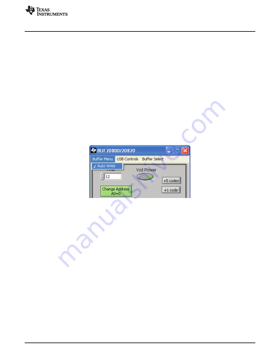
shows the location in the Buffer Menu showing the Auto Write feature enabled. Clicking on the

Auto Write feature again enables/disables the feature, depending on its current state.

Figure 19. Auto Write Feature Enabled

5.2.5

Reset Button

Pressing the Reset button in the BUF20800/20820EVM software performs two functions. The first function
is to call a General-Call Reset for the BUF20800 or BUF20820. The status of the DAC/V

COM

registers after

this General-Call Reset has been used depends on the DUT on the EVM.

If the BUF20800 is in the test board, the channel registers default to 1000000000, or mid-supply.

If the BUF20820 is in the test board, the status of the DAC/V

COM

registers after this General-Call Reset

depends on whether or not the OTP has been programmed. If the OTP has been programmed, the
channel registers are loaded with the last values programmed into the OTP memory. If the OTP memory
has not been programmed, the channel registers will default to 1000000000, or mid-supply.

The second function performed after the reset button is pressed is that a Read DAC call is made to
update the corresponding channel text boxes to the current value for each channel. This function is valid
for both the BUF20800 and the BUF20820 device.

21

SBOU100 – April 2011

BUF20800/20820EVM User Guide and Software Tutorial

Submit Documentation Feedback

© 2011, Texas Instruments Incorporated

Summary of Contents for BUF20800

Page 1: ...20820EVM 8 6 Connecting External Power to the EVM 9 7 Connecting the USB Cable to the USB_DIG_Platform 10 8 Confirmation of USB_DIG_Platform Driver Installation 10 9 BUF20800 20820EVM Default Jumper S...

Page 2: ...COM channels making it ideal for 10 bit source TFT LCD reference drivers The BUF20820 also features programmable OTP memory that allows the user to store the gamma voltages on chip which eliminates th...

Page 3: ...UF20800 product folder or the BUF20820 product folder on the TI web site at www ti com to verify that you have the latest versions of the related software Table 1 BUF20800 20820EVM Kit Contents Item Q...

Page 4: ...ponse Center at 800 477 8924 or the Product Information Center at 972 644 5580 When ordering identify the document by both title and literature number Related Documentation Document Literature Number...

Page 5: ...BUF20800 20820 test board hardware setup is shown in Figure 3 The functionality of the PCB is such that it provides connections to the I2 C interface and general purpose inputs outputs GPIOs on the U...

Page 6: ...nnection 11 N C No connection I2 C clock signal SCL channel 1 can be 12 I2C_SCK_ISO disconnected using a switch I2 C data signal SDA channel 1 can be 13 I2C_SDA_ISO disconnected using a switch 14 N C...

Page 7: ...r download at www ti com The block diagram shown in Figure 4 gives a brief overview of the platform The primary control device on the USB_DIG_Platform is the TUSB3210 Figure 4 USB_DIG_Platform Block D...

Page 8: ...e BUF20800 20820EVM test board The external connections may be the real world system that the BUF20800 or BUF20820 will be incorporated into Figure 5 illustrates the typical hardware connections Figur...

Page 9: ...connect a 6V wall supply to the USB_DIG_Platform board as Figure 6 shows Always connect power before connecting the USB cable If you connect the USB cable before connecting the power the computer will...

Page 10: ...p up indicates that the device is ready to be used The USB_DIG_Platform uses the human interface device drivers that are part of the Microsoft Windows operating system Figure 7 Connecting the USB Cabl...

Page 11: ...cally set to the same position When set to the INT position the signals from the digital supply JMP1 and the digital communication lines JMP2 JMP4 are generated and controlled from the USB_DIG_Platfor...

Page 12: ...connected to jumper JMP5 or whether the LD pin is connected to terminal T3 to allow for an external source to control the latch pin The default INT position connects the LD pin to jumper JMP5 JMP5 L T...

Page 13: ...n the VRAW position the VDUT supply is JUMP17 BUS connected to an external source This configuration allows for any value of VDUT between 3V and 5V 1 Connects the pull up on GPIO to the VDUT supply or...

Page 14: ...the respective values during data transfer until LD sees a low reference such as when JMP5 is set to the L position When JMP5 is set to the L position the LD latch pin is connected to ground which the...

Page 15: ...pter board can be fully evaluated The PowerPAD of this soldered BUF20800 20820 unit is connected correctly allowing the device to dissipate the necessary power while being evaluated CAUTION Only one l...

Page 16: ...the default location is C Program Files BUF208xx and C Program Files National Instruments Following this option two license agreements are presented that must be accepted as shown in Figure 11 After a...

Page 17: ...ing of the OTP register on the BUF20820 The software also permits the user to select either I2 C address Press the About button as shown in Figure 13 to verify that you have the latest version of the...

Page 18: ...nu From Start select All Programs then select the BUF20800 20820EVM program Figure 14 illustrates how the software should appear if the BUF20800 20820EVM is functioning properly Figure 14 BUF20800 208...

Page 19: ...latform 5 2 Using the BUF20800 20820 Software 5 2 1 I2 C Address Selection As mentioned previously in the BUF20800 20820EVM Features section see Section 3 7 jumper JMP6 is used to set the I2 C address...

Page 20: ...mum and minimum levels are then multiplied by the decimal code to determine the DAC voltage The calculation is performed according to Equation 3 3 For example changing the value in the channel 6 cell...

Page 21: ...updated channel that then updates the output voltage When in the Auto Write enabled mode the Write DAC button cannot be pressed with different data in the corresponding channel text boxes than the va...

Page 22: ...folder on your PC It is a good idea to create a directory exclusively for BUF20800 20820 DAC code that is gamma voltage files Enter a unique file name in the File name field to store your BUF20800 20...

Page 23: ...exadecimal DAC codes can be entered in the Code column in the same manner Another method of changing the voltage of a DAC or VCOM channel is through the use of the slider on the main software window T...

Page 24: ...as Figure 23 shows The delay time is the amount of time allowed between loading new configurations into the BUF20800 20820 DUT Use the Single Step Up and Single Step Down buttons to step through the s...

Page 25: ...desired channel output The DAC code and corresponding output value of each channel change automatically This function is similar to the slider present on the primary BUF20800 20820EVM software window...

Page 26: ...he Buffer Model menu As Figure 25 shows pressing the Program OTP All Channels button allows you to program a gamma curve into the nonvolatile memory of the BUF20820 All 18 channels including the VCOM...

Page 27: ...information for the USB_DIG_Platform can be found in the USB_DIG_Platform User s Guide SBOU058 available at the TI web site at http www ti com 6 1 Schematic Figure 26 shows the schematic for the BUF2...

Page 28: ...igure 27 shows the PCB component layout of the BUF20800 20820EVM Figure 27 BUF20800 20820EVM PCB Top Layer Component Side 28 BUF20800 20820EVM User Guide and Software Tutorial SBOU100 April 2011 Submi...

Page 29: ...o Electronics 30 Gold with threaded inserts and board locks 8 4 T1 T2 T3 T5 Terminal Block 5MM 2 Position ED300 2 On Shore Technology Inc 9 1 T4 Terminal Block 5MM 3 Position ED300 3 On Shore Technolo...

Page 30: ...This notice contains important safety information about temperatures and voltages For additional information on TI s environmental and or safety programs please contact the TI application engineer or...

Page 31: ...orized for use in safety critical applications such as life support where a failure of the TI product would reasonably be expected to cause severe personal injury or death unless officers of the parti...

Reviews: