DCIN
PCB Layout Guideline
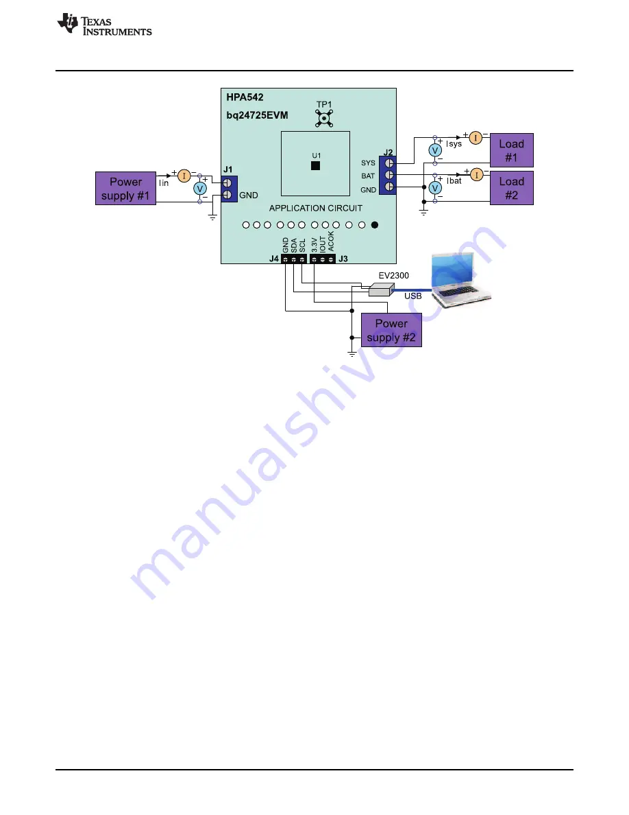
Figure 4. Test Setup for HPA-542
4. Type in "7905" in the Charge Option, and click the Write button. This enables charging.
Measure
→
Ibat = 500 mA
±
100 mA
5. Type in "2944" (mA) in the Charge Current DAC, and click the Write button. This sets the battery
charge current regulation threshold to 2.944 A.
Measure
→
Ibat = 3000 mA
±
300 mA
Measure
→
V(TP(IOUT)) = 340 mV
±
40 mV
6. Enable the output of the Load #1.
Measure
→
Isys = 3000 mA
±
300 mA, Ibat = 1600 mA
±
200 mA, Iin = 4100 mA
±
400 mA
Measure
→
V(TP(IOUT)) = 820 mV
±
100 mV
7. Turn off the Load #1.
Measure
→
Isys = 0 A
±
100 mA, Ibat = 3000 mA
±
300 mA.
8.
2.4.4
Power Path Selection
1. Type in "7905" in the Charge Option, and click the Write button. This disables charging.
2. Replace Load #2 and current meter with PS#3. Make sure a voltage meter is connected across J2
(BAT, GND). Enable the output of the PS #3. Ensure that the output voltage is 10 V
±
500 mV.
Measure
→
Measure
±
V(J2(SYS)) = 19.5 V
±
1 V (adapter connected to system)
3. Turn off PS#1.
Measure
→
V(J2(SYS)) = 10 V
±
1 V (battery connected to system)
Measure
→
V(J2(BAT)) = 10 V
±
1 V (battery connected to system)
3
PCB Layout Guideline
The switching node rise and fall times must be minimized for minimum switching loss. Proper layout of the
components to minimize high-frequency current path loop is important to prevent electrical and magnetic
field radiation and high-frequency resonant problems. The following is a printed-circuit board (PCB) layout
priority list for proper layout. Laying out a PCB according to this specific order is essential.
7
SLUU439A
–
August 2010
–
Revised May 2011
bq24725EVM Evaluation Module
Copyright
©
2010
–
2011, Texas Instruments Incorporated


