EVM Software
21
SNVU564A – July 2017 – Revised August 2017
Copyright © 2017, Texas Instruments Incorporated
Using the BOOST-LP5569EVM Evaluation Module
Enter the desired hex value in the registers (
Current Value
column), perform a bit-wise configuration of
any register fields by double-clicking on the corresponding register bit, or configure a register field by
entering the desired hex value in the
Value
column located under
FieldView
.
FieldView
displays the
description of all fields of the selected register. Each register can be read independently or all registers
can be read at once by using the
Read
or
Read All
button, respectively. The data is written to the
register(s) in one of two ways, depending on the
Update Mode
field selection: In
Immediate
mode, the
register data is written immediately following a
Current Value
, an individual bit, or a
Value
change. In
Deferred
mode, the displayed data is written to all registers on depression of the
Write
button.
Press the
Read All
button to read back all the registers and update the values in this table. If any register
value must be changed, simply double-click on the individual bit values to change the value in this table in
immediate updated mode or press the
Write Register
button to write all the registers at a time if
Deferred
is selected instead of
Immediate
from the drop-down box.
Register settings can be saved in text-file format by selecting
Save Registers
from file menu.
A register settings file in text-file format can be loaded and programmed automatically by selecting
Load
Register
from the file menu.
2.10 Control Menu
The
Control
view is shown when the
Control
icon is clicked, and provides easy ways to control registers
and pin values.
There are five tabs available under the
Control
view:
Manual
,
Program
,
Code Memory
,
Source Edit
, and
Log
. The LP5569 registers are grouped by function with the description of each function being displayed in
the lower right quadrant. When hovering the cursor over a check box, a drop-down dialog pops up a field
describing the settings available. The
Control
view provides immediate mode only, unlike the
Registers
view which also provides deferred mode.
2.10.1
Control View – Common Controls
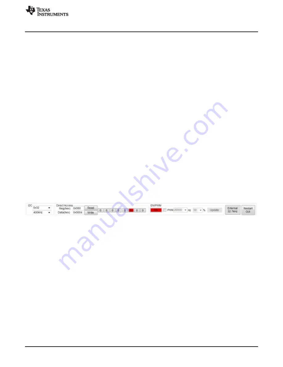
The GUI provides control of I
2
C slave-address selection, direct register access, EN/PWM pin control, and
the external clock that is common to all five control screen tabs.
Figure 27. Common Controls
•
I
2
C Slave Address Selection
–
The I
2
C slave addresses 0x32, 0x33, 0x34, 0x35, 0x40, 0x42, 0x43, 0x44, and 0x45 are available.
The user must ensure that the slave address selected matches the jumper setting on the EVM
ADDR_SEL header (see
•
Direct Register Access
–
Register data can be accessed through the direct access group. The EN pin should be in the high
state before reading or writing data though I
2
C.
•
EN/PWM Pin Control
–
EN pin control. Red color means high, gray means low.
–
The EN pin can be used as PWM, and EVM software supports 500 Hz, 600 Hz, 700 Hz, 800 Hz,
900 Hz, and from 1 kHz to 20 kHz with 1-kHz steps.
–
When PWM is unchecked, the frequency, duty cycle, and update controls are gray (inactive). The
PWM checkbox must be checked to activate the PWM signal from the MSP432 LaunchPad
development kit and enable frequency and duty-cycle updates. The
Update
button must be clicked
after any change to frequency or duty cycle.
•
External Clock Control
–
External clock pin control. Red color means that a 32.7-kHz external clock is operating.


