Texas Instruments BMS034 User Manual Download Page 6

1.3 Recommended Operating Conditions

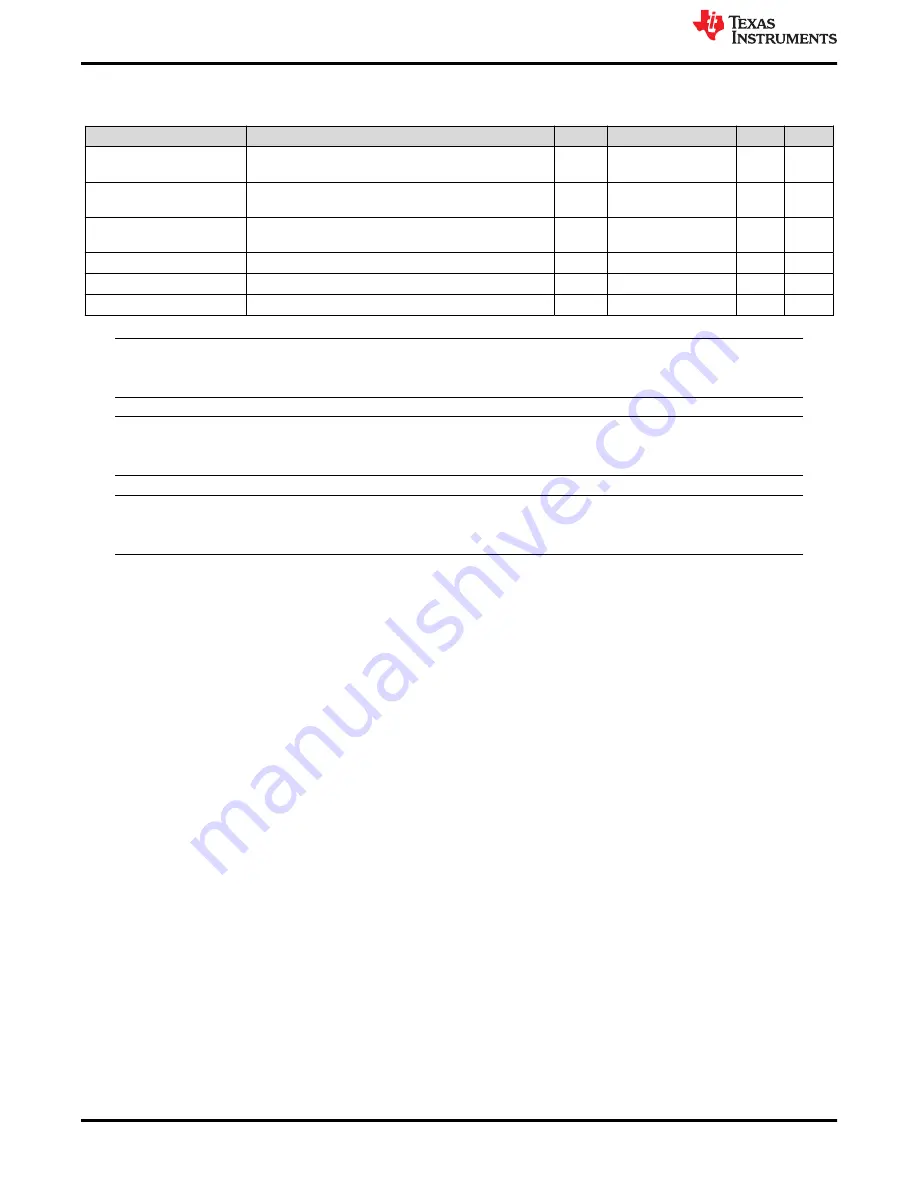
Table 1-4. Recommended Operating Conditions

Description

Min

Typ

Max

Unit

V(VINx) at J1 or J2

Power supply voltage to the external blocking FETs 
which allow power to VBUS pin

3.6

24

V

I(INx) into J1 or J2

Power supply current, which can be limited by charger's 
input current limit feature (IINDPM)

0.01

3.3

A

V(BATTERY) voltage at J5 Battery voltage supported for precharge

2.2

3.8(1S), 7.6(2S), 

11.4(3S), 15.2V(4S)

18.8

V

I(BATTERY) out of/into J5

Battery charge current

0.01

2 (1S, 2S), 1(3S, 4S)

5

A

V(SYS) at J3

System voltage regulation range

3.2

19

V

I(SYS) out of J3

System load current

0

5

A

Note

If hotplugging adaptors with voltage greater than 15 volts, it is reccomended to install RSNUB1, 
CSNUB1, RSNUB2, and CSBUB2 as listed on the schematic.

Note

If hotplugging 4S batteries and a shipFET is installed, it is reccomended to install component CSNUB3 
as listed on the schematic

Note

If hotplugging 4S batteries and a shipFET is not installed, it is reccomended to install component 
DVTS as listed on the schematic.

2 Test Setup and Results

2.1 Equipment

This section includes a list of supplies required to perform tests on the BQ25790EVM.

1.

Power Supplies for VBUS pin:

 Power Supply #1 (PS1): A power supply capable of supplying up to 24 V at 

3 A is required.

2.

Battery Simulator for BAT pin:

 Load #1 (4-Quadrant Supply): A "Kepco" Load, BOP, 20-5M, DC 0 to ±20 V, 

0 to ±6 A (or higher) or a Keithley 2450 3-A sourcemeter. When using both, a 1000-µF or higher, low ESR, 
25-V rated or higher connected at the EVM battery and ground terminals is recommended.
Alternative Option: A 0–20 V/0–5 A, > 60-W DC electronic load set in a constant voltage loading mode in 
parallel with a second power supply can be used. The second power supply is set to a voltage slightly below 
the electronic load's constant voltage setting. When enabled, the charger's charge current then replaces the 
current provided the second power supply.

3.

System load simulator for SYS pin:

Load #2 ( Electronic load set to constant resistance or Resistive Load): 

10 Ω, 5 W (or higher).

4.

Meters:

 (6x) "Fluke 75" multimeters, (equivalent or better).

Alternative Option: (4x) equivalent voltage meters and (2x) equivalent current meters. The current meters 
must be capable of measuring at least 5 A. If used in series between the PS#1, Load#1 or Load#2, the 
meters should be set for manual not auto ranging. Current meters add significant series resistance which 
affects charger performance.

5.

Computer:

 A computer with at least one USB port and a USB cable. A valid internet connection is required 

when using the GUI Composer application.

6.

PC Communication Interface:

EV2300/2400 USB-Based PC Interface Board (when using Battery 

Management Studio) or USB2ANY Interface Adapter (when using the GUI Composer application).

2.2 Equipment Setup

Use the following list to set up the EVM testing equipment. Refer to 

Figure 2-1

 for the test setup connections to 

the EVM:

Introduction

www.ti.com

6

BQ25792EVM, BQ25798EVM and BQ25798BKUPEVM (BMS034) Evaluation 
Module

SLUUCB5E – JUNE 2020 – REVISED JULY 2022

Submit Document Feedback

Copyright © 2022 Texas Instruments Incorporated

Summary of Contents for BMS034

Page 1: ...high temperatures may be present Table of Contents 1 Introduction 3 1 1 EVM Features 3 1 2 I O Descriptions 4 1 3 Recommended Operating Conditions 6 2 Test Setup and Results 6 2 1 Equipment 6 2 2 Equ...

Page 2: ...25798BKUPEVM BMS034A B 005 and BQ25798EVM BMS034A B 003 Schematic Page 2 20 Figure 4 7 BQ25798BKUPEVM BMS034A B 002 Schematic Page 1 21 List of Tables Table 1 1 Device Data Sheet 3 Table 1 2 EVM Conne...

Page 3: ...VM is a complete module for evaluating the BQ25792 8 charger IC in the QFN package Key features of this EVM include Synchronous Switch Mode Buck Boost Charger for 1s 4s Battery Configuration for 5 A C...

Page 4: ...or bypassed ACDRV2 to VAC2 FETs short pins 1 to 2 JP3 VIN1 VAC1 to VBUS bypass connection Connect this when the input protection MOSFET feature is not desired This connects the input source on VIN1 to...

Page 5: ...ct to configure charger default setting to 1S charge regulation voltage 2 A charging current and 750 kHz switching frequency Not Installed JP24 PROG pin setting for 2S 1 5 MHz Connect to configure cha...

Page 6: ...a 1000 F or higher low ESR 25 V rated or higher connected at the EVM battery and ground terminals is recommended Alternative Option A 0 20 V 0 5 A 60 W DC electronic load set in a constant voltage loa...

Page 7: ...re the system voltage as seen from the SYS pins of the charger 9 Install shunts as shown in Table 1 3 Power Supply 1 Load 1 Battery Simulator V V V V V V EV2300 2400 USB V V V V V 4 pin Connector VPMI...

Page 8: ...o the TI Charger GUI landing page From the landing page locate the device desired for evaluation and click Select Device Note that the EVM must be powered and the USB2ANY must be connected to both the...

Page 9: ...ttery Management Studio use the following steps for communications verification 1 In Battery Management Studio select READ REGISTER at the top of the page Device ACK OK should appear at the top of the...

Page 10: ...iption of what the icons on the left side panel mean Figure 2 5 Icon Guide Note If the EVM is powered but not communicating for example does not ACK try updating the USB2ANY firmware to the latest ver...

Page 11: ...BUS Present bit 0 and Power Good bit 3 2 Reinstall the shunt on jumper J17 to enable charge Verify STAT LED D13 is lit 3 Take measurements as follows noting that you may have to adjust the output of t...

Page 12: ...using the PROG pin Jumpers JP24 to JP31 The battery configuration can also be changed using 16 bit register tab Charger Multi bit Registers REG0Ab 7 6 Note that the SYSMIN and charge current charge wi...

Page 13: ...5 Turn on Load 2 output set to CR of 24 6 Take measurements as follows Measure VAC1 PGND TP22 and TP45 12 0 V 0 2 V Measure IAC1 SENSE TP1 and TP2 500 mA 0 10 A 7 Lower the Load 2 CR to 10 8 Take mea...

Page 14: ...r terminal if required 5 Place bulk capacitors for VBUS and BAT pins as close as possible to their respective pins Use at least 2 vias per capacitor terminal if required 6 Place the inductor close to...

Page 15: ...ow the board layout for the BQ2579XEVMs Figure 4 1 BMS034A B Top Layer www ti com Board Layout Schematic and Bill of Materials SLUUCB5E JUNE 2020 REVISED JULY 2022 Submit Document Feedback BQ25792EVM...

Page 16: ...1 Board Layout Schematic and Bill of Materials www ti com 16 BQ25792EVM BQ25798EVM and BQ25798BKUPEVM BMS034 Evaluation Module SLUUCB5E JUNE 2020 REVISED JULY 2022 Submit Document Feedback Copyright 2...

Page 17: ...2 www ti com Board Layout Schematic and Bill of Materials SLUUCB5E JUNE 2020 REVISED JULY 2022 Submit Document Feedback BQ25792EVM BQ25798EVM and BQ25798BKUPEVM BMS034 Evaluation Module 17 Copyright 2...

Page 18: ...Board Layout Schematic and Bill of Materials www ti com 18 BQ25792EVM BQ25798EVM and BQ25798BKUPEVM BMS034 Evaluation Module SLUUCB5E JUNE 2020 REVISED JULY 2022 Submit Document Feedback Copyright 20...

Page 19: ...Figure 4 5 BQ25792EVM BMS034A B 001 and BQ25798EVM BMS034A B 003 Schematic Page 1 www ti com Board Layout Schematic and Bill of Materials SLUUCB5E JUNE 2020 REVISED JULY 2022 Submit Document Feedback...

Page 20: ...2 JP29 1 2 JP28 1 2 JP27 1 2 JP26 3S 3S 4S 4S 1 5MHz 1 5MHz 750kHz 750kHz 1A ICHG 1A ICHG 1A ICHG 1A ICHG AGND 1 2 JP31 1 2 JP33 Green 1 2 D13 1 2 JP32 STAT LED CONNECT STAT 10 0k R39 10 0k R40 10 0k...

Page 21: ...atic Page 1 www ti com Board Layout Schematic and Bill of Materials SLUUCB5E JUNE 2020 REVISED JULY 2022 Submit Document Feedback BQ25792EVM BQ25798EVM and BQ25798BKUPEVM BMS034 Evaluation Module 21 C...

Page 22: ...20 2DS On Shore Technology J5 1 Terminal Block 5 08 mm 3x1 Brass TH 3x1 5 08 mm Terminal Block ED120 3DS On Shore Technology J6 1 Connector Receptacle Micro USB Type B R A Bottom Mount SMT 7 5x2 45x5m...

Page 23: ...0K5FKEA Vishay Dale R32 1 14 0k RES 14 0 k 1 0 1 W AEC Q200 Grade 0 0603 0603 CRCW060314K0FKEA Vishay Dale R33 1 18 0k RES 18 0 k 1 0 1 W AEC Q200 Grade 0 0603 0603 ERJ 3EKF1802V Panasonic R34 1 27 0k...

Page 24: ...D5 D10 0 40V Diode Schottky 40 V 0 38 A SOD 523 SOD 523 ZLLS350TA Diodes Inc D3 D4 D7 D8 0 30V Diode Schottky 30 V 1 A SOD 123 SOD 123 MBR130T1G Diodes Inc D9 0 12V Diode Zener 12 V 300 mW SOD 523 SO...

Page 25: ...reference to BQ25798BKUPEVM and part number 22 Changes from Revision A September 2020 to Revision B December 2020 Page Added BQ25796 and BQ25798 features and data sheet literature numbers 3 Updated d...

Page 26: ...ther than TI b the nonconformity resulted from User s design specifications or instructions for such EVMs or improper system design or c User has not paid on time Testing and other quality control tec...

Page 27: ...These limits are designed to provide reasonable protection against harmful interference in a residential installation This equipment generates uses and can radiate radio frequency energy and if not in...

Page 28: ...instructions set forth by Radio Law of Japan which includes but is not limited to the instructions below with respect to EVMs which for the avoidance of doubt are stated strictly for convenience and s...

Page 29: ...any interfaces electronic and or mechanical between the EVM and any human body are designed with suitable isolation and means to safely limit accessible leakage currents to minimize the risk of electr...

Page 30: ...R DAMAGES ARE CLAIMED THE EXISTENCE OF MORE THAN ONE CLAIM SHALL NOT ENLARGE OR EXTEND THIS LIMIT 9 Return Policy Except as otherwise provided TI does not offer any refunds returns or exchanges Furthe...

Page 31: ...change without notice TI grants you permission to use these resources only for development of an application that uses the TI products described in the resource Other reproduction and display of thes...

Reviews: