


PCB Layout Guidelines
www.ti.com
9
PCB Layout Guidelines
This section provides general practical guidelines for PCB layouts that use various power and ground
traces. Designers should note that these are only “rule-of-thumb” recommendations and the actual results
are predicated on the final layout.
9.1
Power and Ground Circuits
Star trace routing techniques can have a major positive impact on low-level signal performance. Star trace
routing refers to using individual traces that radiate from a signal point to feed power and ground to each
circuit or even device.
9.2
Layout Helpful Hints:
1. Avoid routing traces under the inductor.
2. Use three separate grounds that eventually connect to one point:
(a) Signal or quiet ground (GND2)
(b) Ground for the LM48511 device (GND1)
(c) SW (GND3) (switch ground). This trace for the switch ground carries the heaviest current (3A) and
therefore is the nosiest. Make this trace as wide and short as possible and keep at a distance from
the quiet ground and device ground. Give distance priority to the quiet ground.
10
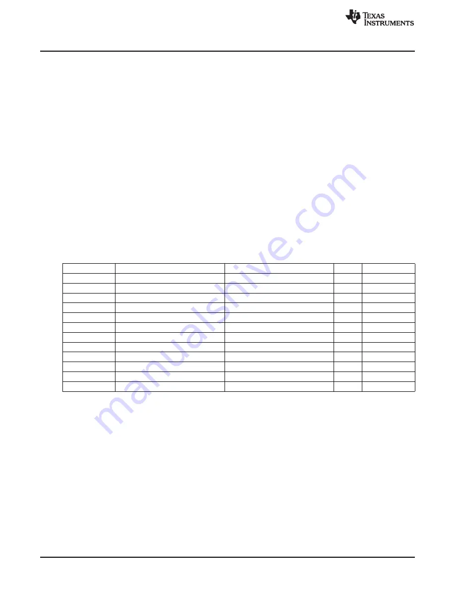
Bill Of Materials
Designator
Description
Footprint
Qty
Value
Cf1
CHIP CAPACITOR GENERIC
CAP 0805
1
470pF
CINA
CHIP CAPACITOR GENERIC
CAP 1210
1
1
μ
F
CINB
CHIP CAPACITOR GENERIC
CAP 1210
1
1
μ
F
Co
CHIP CAPACITOR GENERIC
CAP 1210
1
10
μ
F
Cs1
CHIP CAPACITOR GENERIC
CAP 1210
1
2.2
μ
F
Cs2
CHIP CAPACITOR GENERIC
CAP 1210
1
4.7
μ
F
D1
SCHOTTKY DIODE
DIODE MBR0520 IR
1
L1
IND_COILCRAFT-DO1813P
1
4.7
μ
H
R1
CHIP RESISTOR GENERIC
RES 0805
1
41.2K
R2
CHIP RESISTOR GENERIC
RES 0805
1
13.3K
RINA
CHIP RESISTOR GENERIC
RES 0805
1
150K
RINB
CHIP RESISTOR GENERIC
RES 0805
1
150K
11
Demonstration Board PCB Layout
Figure 3
through
Figure 8
shows the different layers used to create the LM48511SQ demonstration board.
Figure 3
is the silkscreen that shows component locations on the board’s top surface.
Figure 4
is the
metal Top Layer.
Figure 5
is the metal Midlayer 1.
Figure 6
is the metal Midlayer 2.
Figure 7
is the metal
Bottom Layer.
Figure 8
is the silkscreen that shows component locations on the board bottom.
10
AN-1922 LM48511 Evaluation Board
SNAA064C – November 2008 – Revised May 2013
Submit Documentation Feedback
Copyright © 2008–2013, Texas Instruments Incorporated