C8
C12
24.9k
R3
10.0k
R4
0
R9
VCC_S
GND
100nF
C4
100nF
C5
50V
100nF
C10
GND
GND
GND
VCC_S
VCC_S
R6
R2
C2
R1
GND
R5
C6
R7
C9
GND
24.9k
R17
10.0k
R16
0
R11
R14
R19
C21
R18
C20
GND
R15
C16
R13
C13
GND
R10
C14
GND
GND
10.0k
R8
10.0k
R12
GND
VCC_S
100nF
C11
GND
1
J1
1
J2
1
J4
1
J6
1
2
3
4
J3
TP1
IN1-
TP2
IN1+
GND
TP7
IN2+
TP10
IN2-
GND
GND
GND
GND
TP4
GND
GND
TP11
GND
GND
TP8
GND
GND
TP3
OUT1
TP6
OUT2
TP9
GND
GND
TP12
GND
GND
TP5
GND
GND
C1
ALM2403QPWPRQ1
IN1-
1
IN1+
2
SH_DN/OTF
3
IN2+
4
IN2-
5
GND
6
NC
7
NC
8
OUT2
9
VCC
10
VCC
11
VCC
12
OUT1
13
GND
14
A1
A2
Thermal
Shutdown
EN
EN
EN
GND
15
U1
150nF
50V
C3
150nF
50V
C7
150nF
50V
C15
150nF
50V
C17
DNP
DNP
DNP
DNP
DNP
DNP
DNP
DNP
DNP
DNP
DNP
DNP
DNP
DNP
DNP
DNP
DNP
DNP
DNP
DNP
DNP
DNP
DNP
DNP
10uF
C18
100nF
C19
VCC_S
GND
D1
1
2 3
J5
GND
1
2
J7
GND
1
2
3
J8
C22
GND
TP14
GND
GND
VCC_S
TP13
10.0k
R20
10.0k
R21
Modifications
8
SBOU236 – February 2020
Copyright © 2020, Texas Instruments Incorporated
ALM2403-Q1 Evaluation Module
6
Modifications
By default, the ALM2403Q1EVM is populated with both amplifiers set to the inverting configuration.
However, for flexibility, the PCB layout has additional unpopulated passive component footprints, and
additional input connections. These additional component footprints in the layout allow the user to change
the ALM2403Q1 circuit to other common configurations, such as the buffer and noninverting amplifier
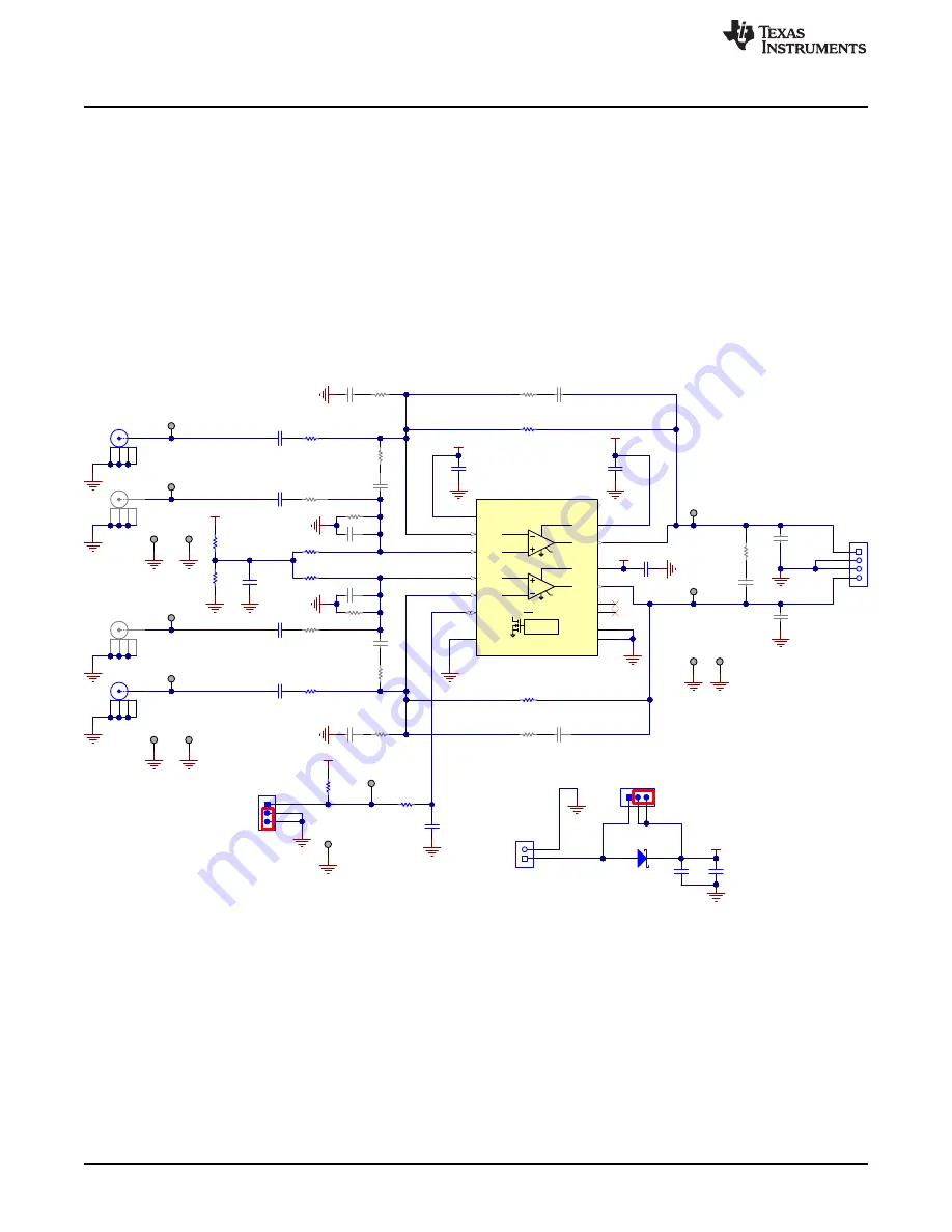
configurations. For a full schematic of the ALM2403Q1EVM, see
.
7
Schematic, PCB Layout, and Bill of Materials
This section contains the schematic, bill of materials, and references for the ALM2403Q1EVM.
7.1
Schematic
illustrates the EVM schematic.
NOTE: DNP components are not populated.
Figure 5. ALM2403Q1EVM Schematic
7.2
PCB Layout
The ALM2403Q1EVM is a four-layer PCB design.
to
show the PCB layer illustrations.
The top layer consists of all signal path traces, and is poured with a solid ground plane. A symmetrical
board layout is used on amplifier 1 and amplifier 2 to keep good performance matching. Decoupling
capacitors C4, C5, and C10 are positioned on the top layer as close as possible to the power supply pins
of the device. The second internal layer is a dedicated solid GND plane. Independent vias are placed at
the ground connection of every component to provide a low-impedance path to ground. The third internal
layer and the bottom layer route the power-supply connections.


