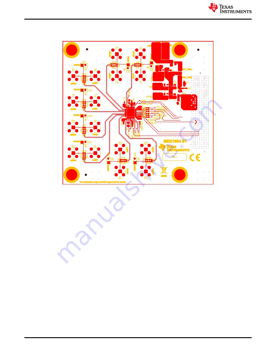
Texas Instruments ADS9817EVM-PDK User Manual Download Page 22

6.3 Layout

Figure 6-5

 shows the top layer and overlay for the EVM PCB layout.

Figure 6-5. ADS9817 PCB Layout Top

Bill of Materials, Schematics, and Layout

www.ti.com

22

ADS9817EVM-PDK Evaluation Module

SBAU416 – NOVEMBER 2022

Submit Document Feedback

Copyright © 2022 Texas Instruments Incorporated

Summary of Contents for ADS9817EVM-PDK

Page 1: ...d circuit board PCB that facilitates connection to a standard FPGA mezzanine card FMC connecter used in many field programmable gate array FPGA kits The EVM PDK eases the evaluation of the ADS9817 dev...

Page 2: ...er Entry and Regulators 8 Figure 5 1 Initial Software Installation 9 Figure 5 2 Installation Process 10 Figure 5 3 Open Device Manager 10 Figure 5 4 Update Driver With Device Manager 11 Figure 5 5 Con...

Page 3: ...ation of the ADS9817 ADC The FMC connecter adapter board as shown in Figure 1 1 facilitates connection to common FPGA kits The TSWDC155EVM controller sold separately requires a separate 5 V 2 A power...

Page 4: ...UI and TSWDC155EVM Power FMC connector Power SMA SMA SMA SMA SMA SMA ADS9817 AIN1M AIN1P AIN8M AIN8P AIN7M AIN7P SMA SMA AIN7M AIN7P SMA SMA AIN7M AIN7P SMA SMA AIN7M AIN7P SMA SMA AIN7M AIN7P SMA SMA...

Page 5: ...44 SMPL_SYNC 45 CS 25 PWDN 32 RESET 31 D0 34 D1 35 D2 36 D3 37 DCLKIN 43 DCLKOUT 33 FCLKOUT 40 SCLK 26 SDI 27 SDO 28 SPI_EN 24 VBIAS 20 NC 38 NC 39 NC 50 NC 51 ADS9817IRSHT U1A AVDD_1V8 21 AVDD_1V8 4...

Page 6: ...he negative input connector can be used to measure the local sensors ground The negative input has a range of 0 3 V Figure 2 2 shows the input connections for a digital interface GND AIN1P AIN1M 0 R4...

Page 7: ...E5 E6 E6 E7 E7 E8 E8 E9 E9 E10 E10 E11 E11 E12 E12 E13 E13 E14 E14 E15 E15 E16 E16 E17 E17 E18 E18 E19 E19 E20 E20 E21 E21 E22 E22 E23 E23 E24 E24 E25 E25 E26 E26 E27 E27 E28 E28 E29 E29 E30 E30 E31...

Page 8: ...provides reverse polarity protection if the connection is miswired Figure 4 1 shows a schematic for various protection circuits 1 2 J17 GND OUT 5 GND 2 IN 1 EN 3 NC 4 TPS7A2050PDBVR U3 5V GND 1 F 16V...

Page 9: ...VM GUI installer from the Tools and Software folder of the ADS9817EVM and run the GUI installer to install the EVM GUI software on your computer Accept all the license agreements and choose the destin...

Page 10: ...using a USB C to USB A cable 2 Open the Windows Device Manager as shown in Figure 5 3 and right click on the WestBridge folder in the Device Manager window and select the Update Driver button see Figu...

Page 11: ...Figure 5 4 Update Driver With Device Manager www ti com EVM Operation SBAU416 NOVEMBER 2022 Submit Document Feedback ADS9817EVM PDK Evaluation Module 11 Copyright 2022 Texas Instruments Incorporated...

Page 12: ...e Initialize USB Power Up Program FPGA and Initialize ads92xx buttons on the Config tab to power up and configure the EVM see Figure 5 8 for details 8 Connect a single ended 5 0 V signal generator 9 P...

Page 13: ...rogram FPGA buttons some status LEDs on the hardware illuminate The power up step takes the longest time approximately 30 seconds After all four buttons are pressed the power on the ADS9817EVM is on a...

Page 14: ...a Finally select the Hanning type window to eliminate spectral leakage in the FFT result When these changes are made press the Start Capture button to collect time domain and frequency domain data Sel...

Page 15: ...and the hits per code then press the GET INL DNL button as shown in Figure 5 9 to run this tool 1 Select INL DNL 2 Select the hits percode for linearity analysis More hits produces more accurate resu...

Page 16: ...Littelfuse D2 1 Green LED Green SMD LED_0805 APT2012LZGCK Kingbright H1 H2 H3 H4 4 Machine Screw Round 4 40 x 1 4 Nylon Philips panhead Screw NY PMS 440 0025 PH B F Fastener Supply H5 H6 H7 H8 4 Stan...

Page 17: ...struments U2 1 6V Low IQ Ideal Diode with Input Polarity Protection DCK0006A SOT SC70 6 DCK0006A LM66100DCKR Texas Instruments U3 1 300 mA ultra low noise low IQ low dropout LDO linear regulator with...

Page 18: ...DGND 46 IOGND 29 IOGND 42 Thermal_Pad 57 REFM 8 REFM 18 REFOUT_2V5 19 REFIO 52 REFM 53 ADS9817IRSHT U1B 10V 1 F C19 10V 0 1 F C20 10V 0 1 F C21 GND GND GND 5V 10V 1 F C15 10V 0 1 F C16 GND GND 10V 0 1...

Page 19: ...0 R34 10k R32 DNP GND GND GND GND GND GND GND 1 2 J19 1 2 J23 1 2 J20 1 2 J24 1 2 J21 1 2 J25 1 2 J22 1 2 J26 1 2 3 4 5 J1 GND 1 2 3 4 5 J2 GND 1 2 3 4 5 J9 GND 1 2 3 4 5 J10 GND 1 2 3 4 5 J3 GND 1 2...

Page 20: ...37 E37 E38 E38 E39 E39 E40 E40 J27E ASP 134486 01 F1 F1 F2 F2 F3 F3 F4 F4 F5 F5 F6 F6 F7 F7 F8 F8 F9 F9 F10 F10 F11 F11 F12 F12 F13 F13 F14 F14 F15 F15 F16 F16 F17 F17 F18 F18 F19 F19 F20 F20 F21 F21...

Page 21: ...DD EN 3 IN 1 NC 4 OUT 5 GND 2 TPS7A2018PDBVR U4 EN 3 IN 1 NC 4 OUT 5 GND 2 TPS7A2018PDBVR U6 SW 1 GND 2 EN 3 FB 4 VOUT 5 VBAT 6 TPS61070DDCR U5 10uH L1 GND 16V 10uF C5 GND 1 96M R2 200k R3 GND 25V 22...

Page 22: ...overlay for the EVM PCB layout Figure 6 5 ADS9817 PCB Layout Top Bill of Materials Schematics and Layout www ti com 22 ADS9817EVM PDK Evaluation Module SBAU416 NOVEMBER 2022 Submit Document Feedback...

Page 23: ...the EVM PCB layout Figure 6 6 ADS9817 PCB Layout Bottom www ti com Bill of Materials Schematics and Layout SBAU416 NOVEMBER 2022 Submit Document Feedback ADS9817EVM PDK Evaluation Module 23 Copyright...

Page 24: ...ther than TI b the nonconformity resulted from User s design specifications or instructions for such EVMs or improper system design or c User has not paid on time Testing and other quality control tec...

Page 25: ...These limits are designed to provide reasonable protection against harmful interference in a residential installation This equipment generates uses and can radiate radio frequency energy and if not in...

Page 26: ...instructions set forth by Radio Law of Japan which includes but is not limited to the instructions below with respect to EVMs which for the avoidance of doubt are stated strictly for convenience and s...

Page 27: ...any interfaces electronic and or mechanical between the EVM and any human body are designed with suitable isolation and means to safely limit accessible leakage currents to minimize the risk of electr...

Page 28: ...R DAMAGES ARE CLAIMED THE EXISTENCE OF MORE THAN ONE CLAIM SHALL NOT ENLARGE OR EXTEND THIS LIMIT 9 Return Policy Except as otherwise provided TI does not offer any refunds returns or exchanges Furthe...

Page 29: ...change without notice TI grants you permission to use these resources only for development of an application that uses the TI products described in the resource Other reproduction and display of thes...

Reviews: