


Analog Interface
7
SBAU315A – July 2018 – Revised June 2019
Copyright © 2018–2019, Texas Instruments Incorporated
ADS9224REVM-PDK
2.3
ADS9224R Internal Reference
The ADS9224R device incorporates an internal 2.5-V band-gap reference and independently matched
reference buffers for each ADC. The internal reference output pin (REFOUT) is decoupled with a 1-µF
capacitor and can be probed at test point TP8. The internally matched reference buffers provide a gain of
1.6384 V/V. These reference buffers generate a high-precision, 4.096-V reference voltage for each ADC
channel at pins REFP_A and REFP_B. These pins are decoupled with 10-µF decoupling capacitors.
Additionally, a mid-reference output (REFby2) is available at test point TP5. This internal REFby2 buffer
provides a common-mode voltage for input amplifiers driving the ADC inputs.
3
Digital Interfaces
As noted in
, the EVM interfaces with the PHI that, in turn, communicates with the computer
using the USB interface. There are two devices on the EVM that communicate with the PHI: the
ADS9224R ADC (over SPI or multiSPI) and the EEPROM (over I
2
C). The EEPROM comes
preprogrammed with the information required to configure and initialize the ADS9224REVM-PDK platform.
After the hardware is initialized, the EEPROM is no longer used.
3.1
multiSPI™ for ADC Digital IO
The ADS9224REVM-PDK supports several interface modes, as detailed in the
. In
addition to the standard SPI modes (single-, dual-, and quad-SDO lines), the multiSPI modes support
single- and dual-data output rates. The PHI is capable of operating at a 3.3-V logic level and is directly
connected to the digital I/O lines of the ADC.
lists the test points available for probing the SPI pins
in both SPI and parallel byte mode.
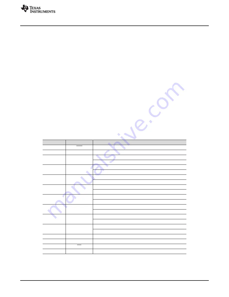
Table 3. SPI Test Points
Designator
Signal
Description
TP1
RST
Asynchronous reset; active low.
TP2
READY/STR
Indicates data-ready or strobe output for data capture.
TP3
SDO-0/0A
SPI mode: data output 0 for channel A.
Parallel byte mode: least significant bit (LSB) from the data byte.
TP4
SDO-1/1A
SPI mode: data output 1 for channel A.
Parallel byte mode: LSB+1 from the data byte.
TP6
SDO-2/2A
SPI mode: data output 2 for channel A.
Parallel byte mode: LSB+2 from the data byte.
TP7
SDO-3/3A
SPI mode: data output 3 for channel A.
Parallel byte mode: LSB+3 from the data byte.
TP9
SDO-4/0B
SPI mode: data output 4 for channel A.
Parallel byte mode: LSB+4 from the data byte.
TP10
SDO-5/1B
SPI mode: data output 5 for channel A.
Parallel byte mode: LSB+5 from the data byte.
TP11
SDO-6/2B
SPI mode: data output 6 for channel A.
Parallel byte mode: LSB+6 from the data byte.
TP12
SDO-7/3B
SPI mode: data output 7 for channel A.
Parallel byte mode: MSB from the data byte.
TP13
SCLK
Clock input pin for the serial interface.
TP14
SDI
Serial data input pin.
TP15
CS
Chip-select input pin; active low.
TP16
CONVST
Conversion start input pin.