Bill of Materials, PCB Layout, and Schematics
www.ti.com
7.2
PCB Layout
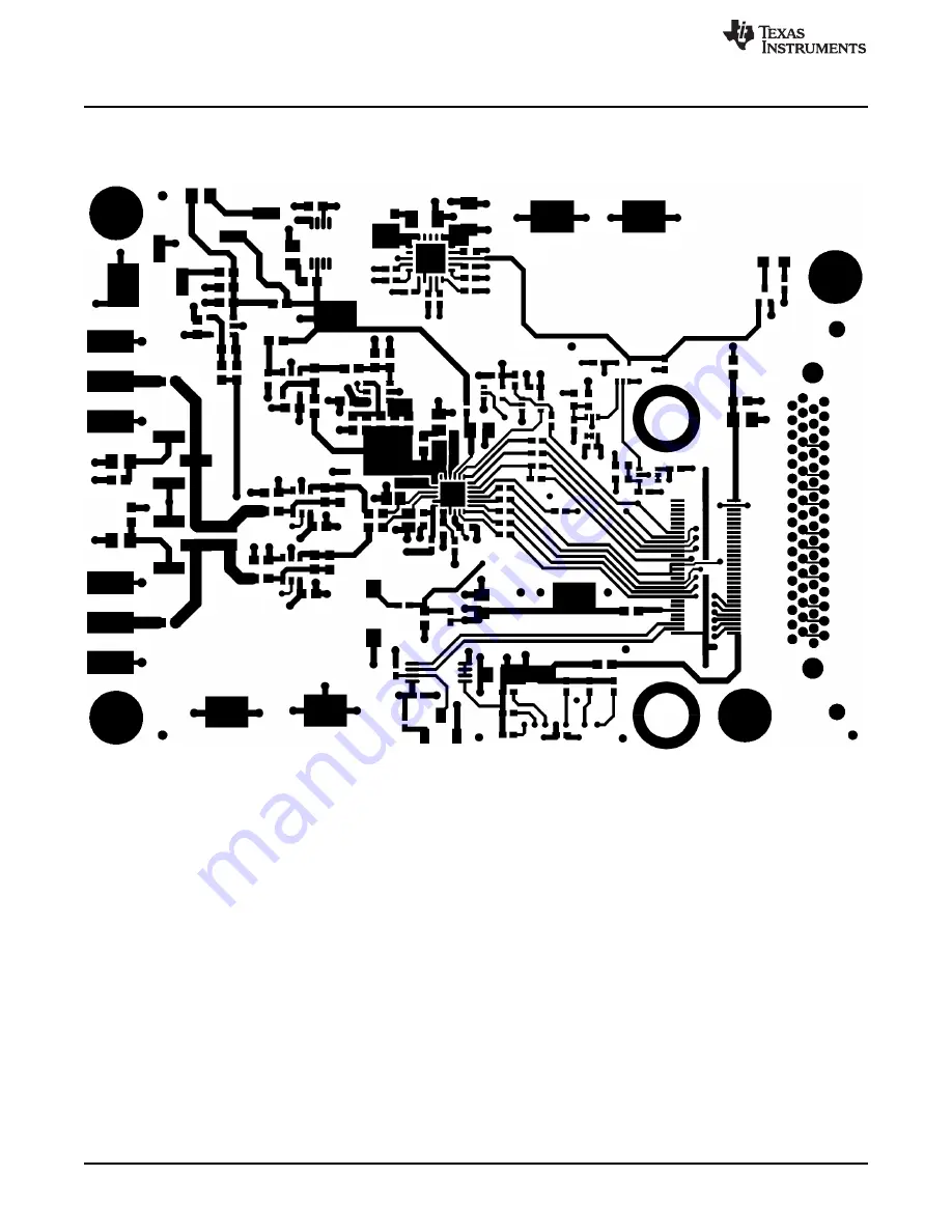
Figure 16
through
Figure 19
illustrate the EVM PCB layout.
Figure 16. ADS9110EVM PCB Layer 1: Top Layer
26
ADS9110EVM-PDK
SBAU249 – October 2015
Submit Documentation Feedback
Copyright © 2015, Texas Instruments Incorporated


