background image

As a Reference Board

5-2

5.1

As a Reference Board

As a reference design, the ADS8402/ADS8412EVM contains the essential
circuitry to showcase the analog-to-digital converter. This essential circuitry
includes the input amplifier, reference circuit, and buffers. The EVM analog
input circuit is optimized for 100-kHz sine wave. Therefore, users may need
to adjust the resistor and capacitor values of the A/D input circuit. In ac-type
applications where signal distortion is a concern, polypropylene capacitors
should be used in the signal path.

5.2

As a Prototype Board

As a prototype board, the buffer circuit consists of resistor pads for configuring
the input as either single-ended or differential input. The input circuit can be
modified to accommodate user prototype needs, whether it be evaluating
another differential amplifier or limiting noise for best performance. The
analog, power, and digital connectors can be made to plug into a standard
0.1 in. breadboard or cables made up to interface directly to an FPGA or
processor.

5.3

As a Software Test Platform

As a software test platform, connectors P1, P2, and P3, plug into the parallel
interface connectors of the 5 - 6K interface card. The 5 - 6K interface card sits
on the C5000 and C6000 digital signal processor starter kit (DSK). The
ADS8402/ADS8412EVM is then mapped into the processor’s memory space.
This card also provides an area for signal conditioning. This area can be used
to install application circuit(s) for digitization by the ADS8402/ADS8412
analog-to-digital converter. See the 5 - 6K interface card user’s guide
(SLAU104) for more information.

The ADS8402/ADS8412EVM provides a simple platform for interfacing to the
converter. The EVM provides standard 0.1-in. headers and sockets to wire into
prototype boards. The user only needs to provide three address lines (A2, A1,
A0) and address valid line (DC_CS) to connector P2. To choose which address
combinations generates RD, CONVST, and RESET, set jumpers as shown in
Table 4 - 2. The recall chip select (CS) signal is not memory-mapped or tied to
P2; therefore, it must be controlled via a general purpose pin or shorted to
ground at J3 pin 1. If address decoding is not required, the EVM provides direct
access to converter data bus via P3 and control via J3.

Summary of Contents for ADS8402

Page 1: ...ADS8402 ADS8412EVM December 2003 Data Acquistion User s Guide SLAU126 ...

Page 2: ...titute a license from TI to use such products or services or a warranty or endorsement thereof Use of such information may require a license from a third party under the patents or other intellectual property of the third party or a license from TI under the patents or other intellectual property of TI Reproduction of information in TI data books or data sheets is permissible only if reproduction ...

Page 3: ... handling or use of the goods Please be aware that the products received may not be regulatory compliant or agency certified FCC UL CE etc Due to the open construction of the product it is the user s responsibility to take any and all appropriate precautions with regard to electrostatic discharge EXCEPT TO THE EXTENT OF THE INDEMNITY SET FORTH ABOVE NEITHER PARTY SHALL BE LIABLE TO THE OTHER FOR A...

Page 4: ...f there is uncertainty as to the load specification please contact a TI field representative During normal operation some circuit components may have case temperatures greater than 60 C The EVM is designed to operate properly with certain components above 60 C as long as the input and output ranges are maintained These components include but are not limited to linear regulators switching transisto...

Page 5: ... Interface Chapter 3 Digital Interface Chapter 4 Power Supply Requirements Chapter 5 Using the EVM Chapter 6 ADS8402 ADS8412 BOM Layout and Schematic Related Documentation From Texas Instruments To obtain a copy of any of the following TI documents call the Texas Instruments Literature Response Center at 800 477 8924 or the Product Information Center PIC at 972 644 5580 When ordering identify this...

Page 6: ...h the limits of computing devices pursuant to subpart J of part 15 of FCC rules which are designed to provide reasonable protection against radio frequency interference Operation of this equipment in other en vironments may cause interference with radio communications in which case the user at his own expense will be required to take whatever measures may be required to correct this interference ...

Page 7: ...e 2 3 3 Digital Interface 3 1 4 Power Supply Requirements 4 1 5 Using the EVM 5 1 5 1 As a Reference Board 5 2 5 2 As a Prototype Board 5 2 5 3 As a Software Test Platform 5 2 6 ADS8402 ADS8412EVM BOM Layout and Schematic 6 1 6 1 ADS8402 ADS8412EVM Bill of Materials 6 2 6 2 ADS8402 ADS8412EVM Layout 6 4 6 3 ADS8402 ADS8412EVM Schematic 6 8 ...

Page 8: ...7 Tables 1 1 Analog Input Connector 1 2 1 2 Solder Short Jumper Setting 1 4 2 1 Pinout for Parallel Control Connector P2 2 1 2 2 Jumper Settings for Decoder Outputs 2 2 2 3 Data Bus Connector P3 2 2 2 4 Pinout for Converter Control Connector J3 2 2 3 1 Power Supply Test Points 3 1 3 2 Power Connector J1 Pinout 3 1 5 1 ADS8402 ADS8412EVM Bill Of Materials 5 2 ...

Page 9: ...1 1 EVM Overview EVM Overview This chapter contains the features of the ADS8402 ADS8412 Topic Page 1 1 Features 1 2 1 2 Introduction 1 2 Chapter 1 ...

Page 10: ...re minimum circuitry to showcase the device under test and plug into prototype systems The onboard decoding circuitry enables the user flexibility to map the A D to different addresses in processor memory The power analog and digital control lines are on standard 0 1 in header socket connectors at the edges of the PWB making it easy to wire into prototype systems for evaluation The EVM has been de...

Page 11: ... signal inverting and noninverting input is 180 degrees out of phase that is level shifted such that the signals levels are always equal to or above zero volts The peak to peak amplitude on each input pin can be as large as the reference voltage See the respective product data sheet for more information Topic Page 2 1 Signal Conditioning 2 2 2 2 Reference 2 3 Chapter 2 ...

Page 12: ...ame Description Inverting input P1 1 P1 2 Noninverting input Reserved N A P1 3 P1 4 N A Reserved Reserved N A P1 5 P1 6 N A Reserved Reserved N A P1 7 P1 8 N A Reserved Pin tied to ground AGND P1 9 P 10 N A Reserved Pin tied to ground AGND P1 11 P1 12 N A Reserved Reserved N A P1 13 P1 14 N A Reserved Pin tied to ground AGND P1 15 P1 16 N A Reserved Pin tied to ground AGND P1 17 P1 18 N A Reserved...

Page 13: ... externally The reference buffer circuit on the EVM is not populated with an amplifier The EVM comes installed with an on chip internal reference tied directly to the reference pin of the converter See Chapter 6 for the schematic Table 2 2 Solder Short Jumper Setting Reference Description Jumper Setting Reference Designator Description 1 2 2 3 SJP1 Not used on the EVM SJP2 On chip internal referen...

Page 14: ...2 4 ...

Page 15: ...s line from processor P2 11 A2 Address line from processor P2 13 P2 15 P2 17 P2 19 INTc Set jumper W3 to select BUSY or inverted signal to be applied to this pin Note All even numbered pins of P2 are tied to DGND The read RD conversion start CONVST and reset RESET signals to the converter can be assigned to two different addresses in memory via jumper settings This allows for the stacking of up to...

Page 16: ... Data Bit 2 P3 7 D3 Buffered Data Bit 3 P3 9 D4 Buffered Data Bit 4 P3 11 D5 Buffered Data Bit 5 P3 13 D6 Buffered Data Bit 6 P3 15 D7 Buffered Data Bit 7 P3 17 D8 Buffered Data Bit 8 P3 19 D9 Buffered Data Bit 9 P3 21 D10 Buffered Data Bit 10 P3 23 D11 Buffered Data Bit 11 P3 25 D12 Buffered Data Bit 12 P3 27 D13 Buffered Data Bit 13 P3 29 D14 Buffered Data Bit 14 P3 31 D15 Buffered Data Bit 15 N...

Page 17: ...gnal Description TP14 BVDD Apply 3 3 V or 5 V See ADC data sheet for full range TP11 AVCC Apply 5 Vdc TP12 VA Apply 7 Vdc Positive supply for amplifier TP13 VA Apply 7 Vdc Negative supply for amplifier 2 Use the power connector J1 and derive the voltages elsewhere The pinout for this connector is shown in Table 4 2 If using this connector set the W1 jumper to connect 3 3VD or 5VD from connector to...

Page 18: ...4 2 ...

Page 19: ...e ADS8402 ADS8412EVM serves three functions 1 As a reference design 2 As a prototype board 3 As a software test platform Topic Page 5 1 As a Reference Board 5 2 5 2 As a Prototype Board 5 2 5 3 As a Software Test Platform 5 2 Chapter 5 ...

Page 20: ...or 5 3 As a Software Test Platform As a software test platform connectors P1 P2 and P3 plug into the parallel interface connectors of the 5 6K interface card The 5 6K interface card sits on the C5000 and C6000 digital signal processor starter kit DSK The ADS8402 ADS8412EVM is then mapped into the processor s memory space This card also provides an area for signal conditioning This area can be used...

Page 21: ...412EVM BOM Layout and Schematic This chapter contains the ADS8402 ADS8412EVM bill of materials the layouts and the schematics Topic Page 6 1 ADS8402 ADS8412EVM Bill of Materials 6 2 6 2 ADS8402 ADS8412EVM Layout 6 4 6 3 ADS8402 ADS8412EVM Schematic 6 6 Chapter 6 ...

Page 22: ...sonic ECG or Alternate ERJ 6ENF49R9V RES 49 9 Ω 1 10 W 1 0805 SMD 10 4 1 nF C3 C5 C11 C23 1206 Kemet or Alternate C1206C102J5GACTU Capacitor 1000 pF 50 V ceramic NPO 1206 11 2 68 pF C34 C35 TH WIMA FKP2 68 100 1 68 pF polypropylene capacitor 12 1 6800 pF C17 TH WIMA FKP2 6800 100 1 6800 pF polypropylene capacitor 13 10 0 01 µF C13 C21 C41 C44 C46 C48 C53 C56 C65 C50 603 Kemet or Alternate C0603C10...

Page 23: ...04DBVR Single inverter gate 35 1 U11 16 TSSOP PW Texas Instruments SN74AHC138PWR 3 line to 8 line decoder demultiplexer 36 3 U5 U6 U7 20 TSSOP PW Texas Instruments SN74AHC245PWR Octal bus transceiver tri state 37 1 5X2X 1 J1 5X2X 1_SM T_socket Samtec TSM 105 01 T D V P 0 025 SMT plug top side of PWB 38 1 6X2X 1 J3 6X2X 1_SM T_plug_ _s k Samtec SSW 106 22 S D VS 0 025 SMT socket bottom side of PWB ...

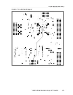
Page 24: ...ADS8402 ADS8412EVM Layout 6 4 6 2 ADS8402 ADS8412EVM Layout Figure 6 1 Top Layer Layer 1 Figure 1 ...

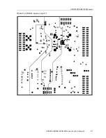
Page 25: ...ADS8402 ADS8412EVM Layout 6 5 ADS8402 ADS8412EVM BOM Layout and Schematic Figure 6 2 Ground Plane Layer 2 ...

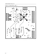
Page 26: ...ADS8402 ADS8412EVM Layout 6 6 Figure 6 3 Power Plane Layer 3 ...

Page 27: ...ADS8402 ADS8412EVM Layout 6 7 ADS8402 ADS8412EVM BOM Layout and Schematic Figure 6 4 Bottom Layer Layer 4 ...

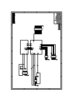
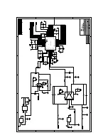
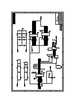
Page 28: ...ADS8402 ADS8412EVM Schematic 6 8 6 3 ADS8402 ADS8412EVM Schematic The following pages contain the schematic for the ADS8402 ADS8412EVM ...

Page 29: ...BUSY B_CS B_RD B_CONVST B_BYTE B_RESET AVCC VA VA BVDD DC_CS A0 A1 A2 INTc Power Digital Buffer J2 B_DB 15 0 DB 15 0 B_DB0 B_DB1 B_DB2 B_DB3 B_DB4 B_DB5 B_DB6 B_DB7 B_DB8 B_DB9 B_DB10 B_DB11 B_DB12 B_DB13 B_DB14 B_DB15 J4 BVDD TP11 TP14 TP13 TP12 CS RD CONVST BYTE RESET B_BUSY ADC Control 1 2 3 4 5 6 7 8 9 11 10 12 J3 1 1 2 2 3 3 4 4 5 5 6 6 7 7 8 8 9 9 10 10 11 11 12 12 13 13 14 14 15 15 16 16 17...

Page 30: ... NI IN C33 1uF R5 100 EXT_REF R4 910 DB 15 0 R11 NI R1 1k TP4 3 1 2 SJP2 C49 10uF C8 0 1uF C13 0 01uF VBD 5 4 8 1 2 VOCM VOUT VOUT 3 6 VCC VCC 7 NC U2 THS4503 1 2 SJP3 IN 1 OUT 2 GND 3 U1 REF3040 5VCC C16 1uF C17 6800pF NC 1 VIN 2 EN 3 GND 4 NC 5 VREF 6 NC 7 NC 8 U9 NI 5VCC C18 0 01uF C45 0 1uF C30 22uF R21 0 R14 100 C61 NI VCC C59 1uF C36 0 1uF VCC C32 0 1uF C60 1uF IN 1 OUT 2 GND 3 U3 REF3040 5V...

Page 31: ...1 A2 A3 A4 A5 A6 A7 A8 B1 B2 B3 B4 B5 B6 B7 B8 VCC GND U7 SN74AHC245PWR VBD C58 0 1uF DB 17 0 DB15 DB14 DB13 DB12 DB11 DB10 DB9 DB8 DB7 DB6 DB5 DB4 DB3 DB2 DB1 DB0 B_DB15 B_DB14 B_DB13 B_DB12 B_DB11 B_DB0 B_DB10 B_DB1 B_DB9 B_DB2 B_DB8 B_DB3 B_DB7 B_DB4 B_DB6 B_DB5 CS RD CONVST BYTE RESET B_BUSY 1 16 2 15 3 14 4 13 5 9 12 6 8 10 11 7 RP2 100 OE DIR A1 A2 A3 A4 A5 A6 A7 A8 B1 B2 B3 B4 B5 B6 B7 B8 V...

Reviews: