


J10
CLK IN
1:4
0.1
P
F
0.1
P
F
121
:
121
:
0.1
P
F
14-bit
ADC
Jp
Jn
0
:
0
:
0
:
0
:
0
:
0
:
0
:
0
:
DNI
DNI
D
N
I
D
N
I
D
N
I
25
:
25
:
0.1
P
F
0.1
P
F
0.1
P
F
0.1
P
F
0
:
10
:
10
:
25
:
25
:
82 nH
10 pF
3
rd
Order Bandpass Filter
RLR Circuit
RLCR Circuit
1:1
1:1
V
CM
Introduction
6
SLAU455B – August 2012 – Revised May 2016
Copyright © 2012–2016, Texas Instruments Incorporated
ADS58H4x (ADS58H40/ADS58H43) EVM
LED D1 is lit indicating the presence of the 6-V supply voltage to the EVM, while LED D2 is lit indicating
the presence of the USB to serial converter power. LEDs D3 and D4 indicate the status of the ADS58H4x
High Resolution Burst Mode.
lists the description of each LED indicator.
Table 5. ADS58H4x EVM LED Indicators
Reference
Designator
Description
D1
When lit, D1 shows the presence of the 6-V (main) power supply
D2
When lit, D2 shows the presence of the USB to serial converter power
D3
When lit, D3 indicates that the ADC is ready to enter trigger mode
D4
When lit, D4 indicates that the ADC is in high resolution burst mode
1.4
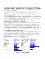
EVM ADC Input Circuit Configurations
shows the ADS58H4x ADC input circuit. The default setup has a dual 1:1 impedance ratio
transformer input circuit, which achieves better phase and amplitude balance of the input signal than is
typically produced by a single transformer input circuit. Third-order bandpass filter component pads are
available for installing bandpass filter components. The default components for the bandpass filter are
either zero
Ω
or open circuit.
The default input termination is 50
Ω
, which is formed by two 25-
Ω
resistors connected to the ADC VCM
node. If the user chooses to use 100-
Ω
termination with the 1:2 impedance transformer, the optional RLR
differential arm can be used to tune the in-band flatness.
The ADC analog input consists of a switched-capacitor-based, differential sample-and-hold (S/H)
architecture. Due to the opening and closing of the sampling glitches, the kick-back noise from the S/H
circuit may affect the ADC performance. Besides the on-chip R-C filter of the ADC input, the external
RLCR circuit provides additional filtering of the glitches. The default RLCR components have been
optimized for input bandwidth centered at 185 MHz. For additional RLCR components of different center
frequencies, refer to the ADS58H40 datasheet (
Figure 4. ADS58H4x ADC Input Circuit
shows the ADS58H4x clock input circuit. The clock signal goes through the 1:4 impedance ratio
transformer increasing the clock amplitude by two (1:4 impedance ratio equals to 1:2 voltage ratio). The
two 121-
Ω
resistors will impedance transform back to the primary side as 50-
Ω
load impedance for the
signal source generator. For ADC evaluation, set the signal generator output to 10 dBm.
Figure 5. ADS58H4x Clock Input Circuit


