


ADS126xEVM Software
•
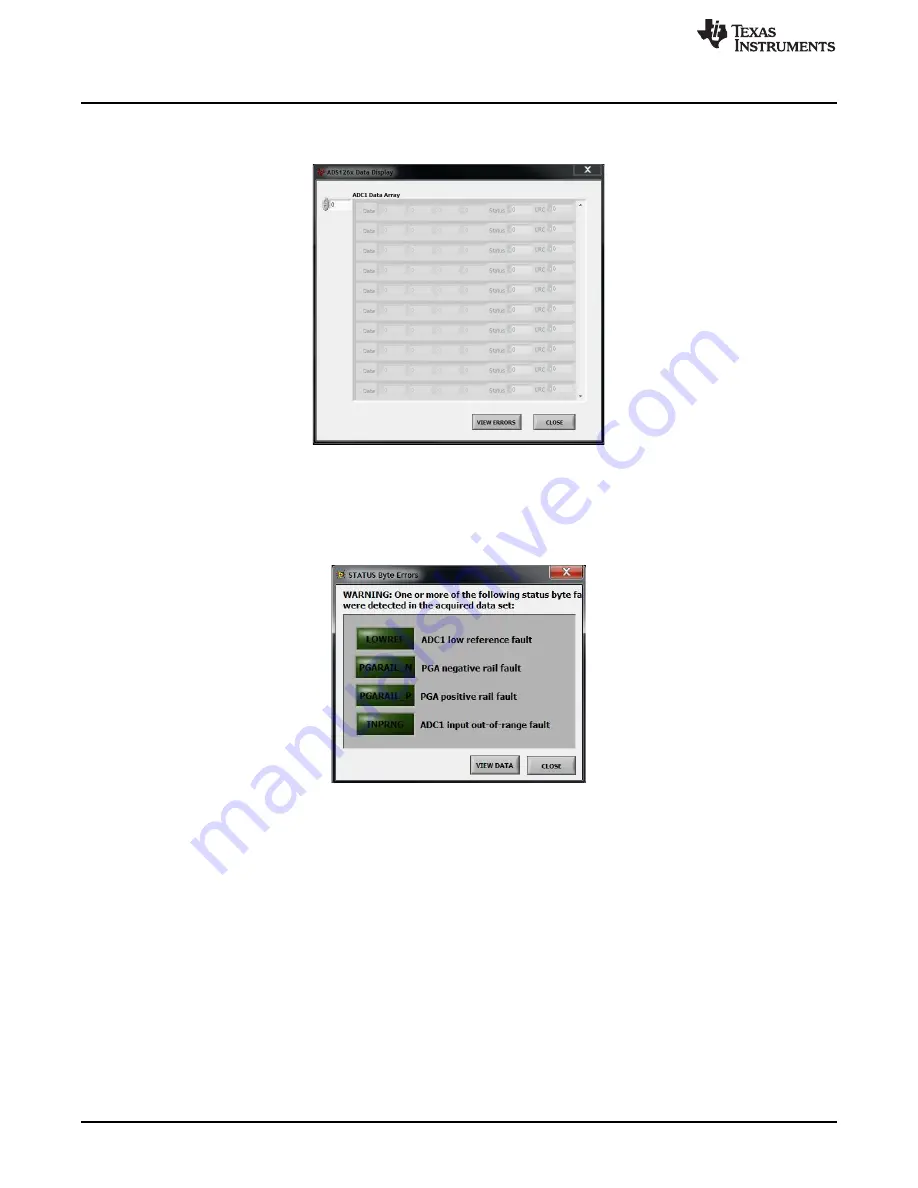
View Data
reveals a data monitor that shows the raw ADC codes along with the STATUS and
CHECKSUM/CRC bytes, as shown in
Figure 27. Data Monitor Window
•
View Errors
reveals a STATUS byte error indicator that ORs all of the STATUS byte error flags to
check if any errors occurred in the previous acquisition, as shown in
. This window
automatically appears when an error flag is found in the acquired data set. Switching to the
View Data
window is useful to see when this error first appeared in the collected data.
Figure 28. Status Byte Error Pop-up
30
ADS126xEVM-PDK
SBAU206 – April 2015
Copyright © 2015, Texas Instruments Incorporated