background image


Application Note P4097 


© TeraTron GmbH 

Page 16 of 21 

V1.1, 07.06.01 

 
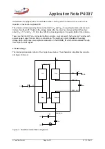
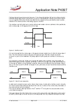
The figure above shows how to enter the value “1” into the serial interface. IN has to be high at least t

S


before the rising edge of CLK. The value for t

S

 is given in the datasheet. If this time is chosen to small 

or even negative (CLK before IN) the data might not be accepted or the serial interface reset could be 
activated. The relative position of the falling edges is uncritical. 
 
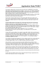
The interface reset with which every serial communication starts is done as defined in the specification 
when a rising edge on IN happens while CLK is high. 
 

tres

CLK

ts

Int_Res

IN


Figure 9.: Interface reset 

 
It is recommended that the rising edge on IN appears at least a settle time of t

s

 after the rising edge of 

CLK. The internal reset is active as long as both signal are high. This time should exceed the 
minimum t

res

 given in the datasheet. The falling edges of both signals are uncritical, it can have any 

order. 
 
It is necessary to start each writing to the serial shift register with a interface reset. By mistake the 
P4097 shift register and the connected µController could not be in phase due to EMI or ESD influence. 
In this case the written or read information would be wrong and it is difficult for the µController to figure 
this out. For that reason the P4097 is designed to be synchronized at each serial transmission with the 
interface reset. 
 

.

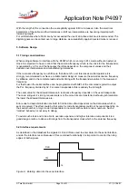
Data 1

.

Reset

.

CLK

Reset

Clock 1

Clock 2

IN


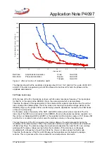
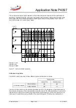
Figure 10.: Start of communication 

 
A valid serial command to power up the chip is shown below. It starts with a interface reset to bring the 
IC in the command state. Because the IN pin has to be low to achieve this a momentary modulation of 
the antenna driver can not be avoided. 
The In pin should be pulled high between the 9

th

 and the 12

th

 clock pulse to avoid modulation at the 

end of data transmission. 
 
The pause between the first 8 bits which are input for the chip and the last 3 bits which are the output 
should be made longer as shown as due to the analog settle time the outputted data might be wrong. 

Summary of Contents for P4097

Page 1: ...ole or in part is prohibited without the prior written consent of the copyright owner The information presented in this document is believed to be reliable and may be changed without notice No liability will be accepted by the publisher for any consequence of its use The publication does not convey nor imply any license under patent or other industrial or intellectual property rights by TeraTron G...

Page 2: ...onsiderations 4 3 2 Power Supply 5 3 3 Filter design 6 3 4 Phase Lock Loop 8 3 5 µC Interface 9 3 6 Active antenna interface 9 3 7 Printed circuit board 9 3 8 EMI Filter 10 3 9 Antenna diagnosis 11 4 Antenna Design 13 5 Software Design 15 5 1 Timing considerations 15 5 2 Interface requirements 15 5 3 Modes of operation 17 5 4 Typical Schematic 20 ...

Page 3: ...ances Furthermore the chip has been designed to support both active and intelligent antenna The difference is the proximity of the controlling µC either it sits close to the P4097 on the same PCB or it is connected via a wiring harness where the number of wires is important and should be minimized Controlled by a serial interface the chip incorporates a power down mode as well as diagnostic capabi...

Page 4: ... too small If the resonance frequency of the transponder and the resonance frequency of the antenna are different the coupling factor between both coils becomes complex This means that the modulated signal is phase shifted against the carrier signal If this phase shift reaches 90 the signal can not be demodulated with a simple peak detector any more as the carrier is being pure phase modulated wit...

Page 5: ...n and can especially in the frequency range of transponder communication not be distinguished from data send by the transponder To get a feeling for the supply voltage rejection of the circuit as there will be always a certain amount of ripple because of non perfect components for a typical configuration the drop of the DEMOD_IN peak voltage is 50mV if the VDD is decreased by 62 5mV The transponde...

Page 6: ...n the quality factor of the antenna Take care that the OUT pin connected buffers or similar must not switch high currents Together with a weak power supply this can form a resonant loop The switched current modulates the supply voltage which can be seen as amplitude modulation on the DEMOD_IN which is demodulated through the chip to the OUT signal 3 3 Filter design The internal demodulation chain ...

Page 7: ...PSK are given in the datasheet When the external clock mode is used this capacitor is not needed and the CF pin should be connected to ground The gain of the involved amplifiers can be selected by using bit 6 and bit 7 of the serial shift register The influence of different gains should be tested by qualification In general the sensitivity is increased with higher gains but the chance of signal cl...

Page 8: ...n to pin spacing For the same reason the polarity of the ANT1 and ANT2 antenna driver pins is important The PLL locks only if the ANT2 pin is connected to the DEMOD_IN pin via the series resonance capacitor not the via the coil Swapping ANT2 and ANT1 or the capacitor and the inductor causes a 180 phase shift and the PLL is not able to lock which means the antenna is driven on the wrong frequency T...

Page 9: ...Connected directly to a µController the rise time should never cause a problem if a direct connection without additional filter capacitors is chosen 3 6 Active antenna interface When the IN and OUT pin are connected together to form with the CLK signal a two wire interface this configuration is called active antenna It is advantageous if the antenna interface is a stand alone unit without a µContr...

Page 10: ... The capacitor should be located close to the chip and the tracks should be short and not close to other traces with fast changing voltage levels The antenna connection if an external antenna is used should be bypassed with two small ceramic capacitors to ground close to the connector This suppresses high frequency voltages to ground which are picked up by the wiring harness and reduces the radiat...

Page 11: ...oth output stages are tested internally for correct voltage levels The driven voltage level and the actual voltage level at the output pin are compared each cycle and the output stage is switched into tri state mode when the output does not reach the assumed voltage This feature protects the P and N channel driver transistor against destruction by short circuit to VSS or VDD The occurrence of thes...

Page 12: ... circuit of ANT2 to VSS 1 1 1 Short circuit of ANT2 to VDD 1 1 1 Broken connection to ANT1 0 1 1 Broken connection to ANT2 0 1 1 Capacitor value too large 0 X 1 Capacitor value too small 0 X 1 Inductor value too large 0 X 1 Inductor value too small 0 X 1 Loop resistance value too large 0 0 0 Loop resistance value too small X 1 0 Antenna voltage is being modulated no failure 0 1 0 The X s are showi...

Page 13: ...esis losses Furthermore the resistive losses are the sum of the copper resistance of the antenna possibly the parasitic resistance of EMC coils and the resistance of the antenna driver given in the datasheet as RAD For measuring the value of Q the voltage over the inductor or the capacitor can be used The formula is given as DD L V Q V Π 4 ˆ Not only the voltage over C and L are linear dependant f...

Page 14: ... antenna voltages This makes it easier and less expensive to find the appropriate electronic components and results in a smaller division factor for the DEMOD_IN voltage Therefore the modulation ratio is kept larger To achieve the lowest cost for the antenna the needed resistance for the desired quality factor could be integrated as copper resistance in the antenna However the copper resistance ha...

Page 15: ... with the transponder relative to the measured frequency For that reason the serial interface can be programmed with bit 3 of the command register to output the PLL frequency divided by 32 For some transponders this is already the bit length The exact value for the allowed tolerance in resonance frequency depends on the used transponder The more stringent it s timing requirements is or the more bi...

Page 16: ...re uncritical it can have any order It is necessary to start each writing to the serial shift register with a interface reset By mistake the P4097 shift register and the connected µController could not be in phase due to EMI or ESD influence In this case the written or read information would be wrong and it is difficult for the µController to figure this out For that reason the P4097 is designed t...

Page 17: ... Channel 2 IN Channel 3 ANT2 Figure 11 Serial command sequence 5 3 Modes of operation The P4097 is able to be used in three different system architectures or modes Clock source Internal PLL External clock Direct Interface yes yes µController location Active Antenna yes no The clock for the antenna can be internally generated by a PLL The frequency is then determined by the resonance frequency of t...

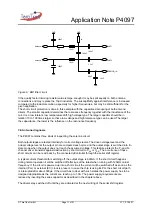
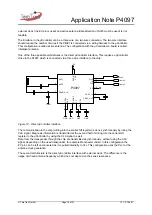
Page 18: ... 11 14 15 16 VSS CLK ANT1 DVDD DVSS ANT2 VDD DEMOD_IN CDEC_OUT CDEC_IN CAGND OUT IN CF CDC EC from µC GND from µC to µC Figure 12 Direct µController interface The communication to the chip writing into the serial shift register is done synchronously by using the CLK signal Diagnosis information is transmitted at the second half of writing into the serial shift register to the µController by using ...

Page 19: ...he additional capacitance of the trace and the input should not be disregarded to achieve a stable start up The input capacitace is given in the datasheet Capacitive coupling in of high frequency signals must be avoided Any jitter on this signal reduces the system performance µController using a PLL for clock generation have to be checked carefully on their clock signal stability The CF pin is con...

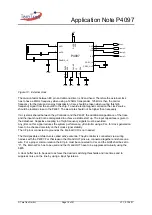
Page 20: ...GND OUT IN CF CDC EC GND 5V 12V Figure 14 Active antenna Because the OUT pin can not be switched to tri state a wired or connection must be used A logic low signal at the OUT pin should not influence the voltage level on the bi directional communication line If the OUT pin is switched to low the line is used as input 5 4 Typical Schematic A typical circuit for interfacing a transponder may look li...

Page 21: ... 9 13 12 11 15 14 16 VSS CLK ANT1 DVDD DVSS ANT2 VDD DEMOD_IN CDEC_OUT CDEC_IN CAGND OUT IN CF CDC EC C5 1 5nF C1 100pF to µC from µC L1 10uH GND C9 100nF C3 100pF R1 10R C8 150nF C10 10nF C7 1nF GND GND Figure 15 Typical application schematic The data of the connected antenna coil are L 1070µH and R 65Ω at 125kHz This includes the cable and the eddy current losses of the lock cylinder ...

Reviews: