background image


15 

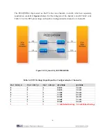
Table 3-5 SW2 Settings (Input Equalizer Configuration for Channel B) 

Pin 4    SEL0_B 

Pin 5    SEL1_B 

Pin 6    SEL2_B 

@1.25GHz 

@2.5GHz 

0.5dB 

1.2 dB 

0.6dB 

1.5 dB 

1.0 dB 

2.6 dB 

1.9 dB 

4.3 dB 

2.8 dB 

5.8 dB 

3.6 dB 

7.1 dB 

5.0 dB 

9.0 dB 

7.7 dB(Default Setting)  12.3 dB(Default Setting) 

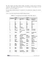
The  SW2  pin  7  connects  to  the  PI2EQX5904  RXD_A  pin,  while  SW2  pin  8  connects  to 
PI2EQX5904 RXD_B pin. These 2 pins are used to control channel A & B Receiver Detect Enable 
function. Automatic Receiver Detection is a feature that can set the number of active channels. By 
sensing  the  presence  of  a  load  device  on  the  output,  the  channel  can  be  automatically  enabled  to 
operate. 
When setting the RXD_A or RXD_B to a high level, Automatic Receiver Detection will be enabled. 
Please refer the datasheet of PI2EQX5904 for more settings.   

Table 3-6 SW2


Settings (Receiver Detect Function Enable for CH_A & CH_B)


Pin 7    RXD_A 

Pin 8    RXD_B 

Receiver Detect Function Enable 

1


CH_A & CH_B Receiver Detect 

Enable (Default Setting)


CH_A Receiver Detect Enable 

CH_B Receiver Detect Disable 

CH_A Receiver Detect Disable 

CH_B Receiver Detect Enable 

CH_A & CH_B Receiver Detect 

Disable 


3

3

.

.

4

4


L

L

E

E

D

D

s

s


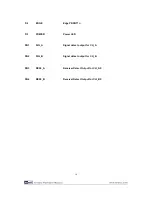
The PCA includes status LEDs, Please refer 

Table 3-7 

for the status of the LED indicator.


Board 

Reference 

LED name 

Description 

D1 

CBL 

Cable PRSNT1n 

Summary of Contents for PCA

Page 1: ......

Page 2: ...Chapter 2 Architecture 4 2 1 Layout and Components 4 2 2 Block Diagram of the PCA Board 5 Chapter 3 Board Components 7 3 1 PCIe Edge Connector 7 3 2 PCIe Cable Connector 9 3 3 Switches 12 3 4 LEDs 15 Chapter 4 Appendix 17 4 1 Revision History 17 4 2 Copyright Statement 17 ...

Page 3: ...CA can provide programmable equalization amplification and de emphasis for PCIe transceiver signal by using 8 select bits It is also available to optimize performance over a variety of physical mediums by reducing Inter symbol interference 1 1 1 1 F Fe ea at tu ur re es s Figure 1 1 shows a photograph of the PCA Figure 1 1 Exterior View The key features of the card are listed below ...

Page 4: ...Adjustable receiver equalization Adjustable transmitter amplitude and de emphasis 1 1 2 2 G Ge et tt ti in ng g H He el lp p Here is information of how to get help if you encounter any problem Terasic Technologies Tel 886 3 550 8800 Email support terasic com ...

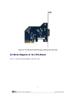
Page 5: ... 2 1 1 L La ay yo ou ut t a an nd d C Co om mp po on ne en nt ts s The picture of the Terasic PCIe x4 Cable Adapter PCA is shown in Figure 2 1 and Figure 2 2 It depicts the layout of the board and indicates the locations of the connectors and key components Figure 2 1 The PCA Card PCB and Component Diagram top view ...

Page 6: ... Figure 2 2 The PCA Card PCB and Component Diagram bottom view 2 2 2 2 B Bl lo oc ck k D Di ia ag gr ra am m o of f t th he e P PC CA A B Bo oa ar rd d Figure 2 3 shows the block diagram of the PCA card ...

Page 7: ...6 Figure 2 3 Block Diagram of PCA ...

Page 8: ...tor is used to connect the PCA with PC motherboard PCIe slot as show Figure 3 1 and Figure 3 2 Figure 3 1 PCA Edge Connector Figure 3 2 Plug the PCA into the PCIe slot of the Motherboard The pins are numbered as shown in Table 3 1 with side A on the top of the center line on the solder side of the board and side B on the bottom of the centerline on the component side of the board ...

Page 9: ... NC NC NC 3 NC NC NC NC 4 GND Ground GND Ground 5 NC NC NC NC 6 NC NC NC NC 7 GND Ground NC NC 8 VCC3P3 3 3V Power NC NC 9 NC NC VCC3P3 3 3V Power 10 3 3VAUX 3 3 V Auxiliary Power VCC3P3 3 3V Power 11 WAKE NC PERSTn Fundamental Reset Mechanical Key 12 RSVD Reserved GND Ground 13 GND Ground REFCLK Reference clock differential pair 14 PETp0 Transmitter differential pair Lane 0 REFCLK 15 PETn0 GND Gr...

Page 10: ...NT2n Hot Plug presence detect GND Ground 32 GND Ground RSVD Reserved 3 3 2 2 P PC CI Ie e C Ca ab bl le e C Co on nn ne ec ct to or r A PCIe cable connector is used to connect the PCIe x4 Cable and PCA cable connector Connect the adapter by using a PCIe x4 Cable as show Figure 3 3 Figure 3 3 PCIe x4 Cable and PCA To purchase the PCIe x4 Cable please refer the url PCIe_Cable terasic com Figure 3 4 ...

Page 11: ...ter Lane 0 A3 PETn0 Differential PCI Express transmitter Lane 0 A4 GND Ground reference for PCI Express transmitter Lanes A5 PETp1 Differential PCI Express transmitter Lane 1 A6 PETn1 Differential PCI Express transmitter Lane 1 A7 GND Ground reference for PCI Express transmitter Lanes A8 PETp2 Differential PCI Express transmitter Lane 2 A9 PETn2 Differential PCI Express transmitter Lane 2 A10 GND ...

Page 12: ... to slavetype downstream subsystems B1 GND Ground reference for PCI Express transmitter Lanes B2 PERp0 Differential PCI Express receiver Lane 0 B3 PERn0 Differential PCI Express receiver Lane 0 B4 GND Ground reference for PCI Express transmitter Lanes B5 PERp1 Differential PCI Express receiver Lane 1 B6 PERn1 Differential PCI Express receiver Lane 1 B7 GND Ground reference for PCI Express transmit...

Page 13: ... for wakeup events optional B19 CPERSTn Cable PERSTn 3 3 3 3 S Sw wi it tc ch he es s The PCA contains x2 and x8 switches that allow configuration of the PCA PCIe mode SW1 equalization and de emphasis SW2 The two switches SW1 and SW2 are located on top of the front side of the PCA card Figure 3 5 show the location of the board Figure 3 5 Switches ...

Page 14: ...13 Figure 3 6 show the SW1 settings Table 3 3 SW1 Settings Pin 2 Pin 1 PCIe Mode x1 x4 UP UP NULL UP Down x1 Down UP x4 Default mode Down Down NULL Figure 3 7 Show the SW2 Settings ...

Page 15: ...ttings on Equalizer Configuration for channel A or channel B Figure 3 8 CH_A and CH_B of PI2EQX5904 Table 3 4 SW2 Settings Input Equalizer Configuration for Channel A Pin 1 SEL0_A Pin 2 SEL1_A Pin 3 SEL2_A 1 25GHz 2 5GHz 0 0 0 0 5dB 1 2 dB 0 0 1 0 6dB 1 5 dB 0 1 0 1 0 dB 2 6 dB 0 1 1 1 9 dB 4 3 dB 1 0 0 2 8 dB 5 8 dB 1 0 1 3 6 dB 7 1 dB 1 1 0 5 0 dB 9 0 dB 1 1 1 7 7 dB Default Setting 12 3 dB Defa...

Page 16: ...hannels By sensing the presence of a load device on the output the channel can be automatically enabled to operate When setting the RXD_A or RXD_B to a high level Automatic Receiver Detection will be enabled Please refer the datasheet of PI2EQX5904 for more settings Table 3 6 SW2 Settings Receiver Detect Function Enable for CH_A CH_B Pin 7 RXD_A Pin 8 RXD_B Receiver Detect Function Enable 1 1 CH_A...

Page 17: ...2 EDGE Edge PRSNT1n D3 POWER Power LED DN1 SIG_A Signal detect output for CH_A DN2 SIG_B Signal detect output for CH_B DN3 RX50_A Receiver Detect Output for CH_A0 DN4 RX50_B Receiver Detect Output for CH_B0 ...

Page 18: ...is si io on n H Hi is st to or ry y Version Change Log V1 0 Initial Version Preliminary V1 1 Delete the chapter of TR4 demo 4 4 2 2 C Co op py yr ri ig gh ht t S St ta at te em me en nt t Copyright 2012 Terasic Technologies All rights reserved ...

Page 19: ...Mouser Electronics Authorized Distributor Click to View Pricing Inventory Delivery Lifecycle Information Terasic P0113 ...

Reviews: