TM 9-6625-474-14&P-3
is made active The bcd output data is demultiplexed via
the time slot lines driving the eight LED’s in the display
(schematic 8). The bcd output codes area also converted to
seven segment information by U1610.
Decimal Point and Annunciator Encoder
T w o p r o g r a m m a b l e r e a d o n l y m e m o r y ( P R O M )
devices, U1200 and U1300, are used to accept the setting
i n f o r m a t i o n f r o m t h e F U N C T I O N a n d A V G S / T I M I N G
switch circuits on schematic 9. This information lets the
PROMS know what function and timing point the instru-
ment is in so that they can, in turn, select which decimal
point and annunciator should be illuminated. The annun-
ciators are the GHz/nSEC,
KHz/mSEC, and
Hz/SEC indicator lights.
The decimal point data from the PROMS is fed to pins 9,
10, and 11 of U1400, a one-of-eight selector/multiplexer.
Integrated circuit U1400 is used as a single pole, seven
position switch that switches the proper time slot pulse
(TS1 through TS7) to the decimal point scanned lines,
pins 6 and 5 of U1400. Pin 5 will havea positive pulse and
pin 6 a negative pulse for the decimal point scanned
information.
Decimal point information is not displayed in the
TOTALIZE A mode. Pin 9 of U1422C and pin 13 of U1612F
are set low, and pin 10 of U1422C is set high forthis mode.
This coding deselects and turns off both PROMS at pin 15
(high) and deselects U1400 at pin 7 (high).
There are four sets of decimal point and annunciator
information contained in the two PROMS. These four
sections are selected by the ADE and ADF lines as shown
in Table 3-1.
PROM SELECTION CODE
D i s p l a y
The eight digit LEDs are common cathode displays,
with the time slot pulses (TS1 through TS8) scanning pin 6
on each digit; DS1002 is the most significant digit and
DS1305 is the least significant digit. All of the seven
segment and decimal point information is paralled. For
leading zero suppression during the scanning cycle, the
display is blanked (seven segment information is
missing)
until the first non-zero digit or decimal point is en-
countered.
The GATE and OVERFLOW lights, CR1011 and CR1012,
are driven by current limit resistors, R1011 and R1012. A
single current limiting resistor, R1009, is used for the four
annunciator lights because only oneofthem is illuminated
at any given time.
Switching Logic
(FUNCTION, AVGS/TIMING)
The FUNCTION switching logic for S1810 is on the A12
A u x b o a r d ( t o p h a l f o f s c h e m a t i c ) , w h i l e
t h e
AVGS/TIMING switching logic for S1010 is on the A14
Main board (lower half of schematic). A simplified logic
pattern for S1810 is located on schematic 3 and the logic
pattern for
S1010 is located on schematic 6.
The switch wafer positions for the FUNCTION switch
are drawn in-line, horizontally with one wafer position
offset slightly to indicate reset between detents. The same
type of pattern is drawn for the AVGS/TIMING switch,
S1010.
Integrated circuits U1611D and U1611B are used to
reset the Time A
BGenerator
when either measurement
mode for that function is activated or whenever the clear
pulse occurs on pin 6 of U1611B.
Pin 8 of U1600D is set low for the modes that use the
10 MHz Time Base clock as the direct Count Input to the
Decade Accumulators. Pin 10 of U1611C is set low for
those modes that use the Channel A signal as the direct
Count Input. The remaining logic gates, along with the
actual grounded positions of the FUNCTION switch,
control the signal paths discussed under the Block
Diagram discussion and the
discussion for the Signal
Routing and Gate Generator circuits.
The ADE control line (U1611A, pin 3) and the ADFline
(U1600E, pin 10) areused toaddressthetwo PROMs in the
Decimal Point and Annunciator Encoder circuits (see
The tenth position of the FUNCTION switch is used for
the TOTALIZE A and TIME MANUAL modes. The desired
Summary of Contents for DC503a
Page 1: ...e x _ 1 v w W i L ...
Page 16: ...DC 503A DC 503A Universal Counter Timer REV A FEB 1981 XIV ...
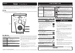
Page 27: ...Fig 2 2 Controls and connectors Operating Instructions DC 503A 2977 fli English 2 3 ...
Page 39: ...Fig 2 2 Commandes et prises Instructions d utilisation DC 503A French 2 3 ...
Page 51: ...Abb 2 2 Bedienungselemente and Anschliisse Bedienungsanleitung DC 503A German 2 3 ...
Page 63: ...Fig 2 2 Controls and connectors Operating Instructions DC 503A 2971 01 Japanese 2 3 ...
Page 125: ...Fig 8 2 Auxiliary Board A12 Assy ADJUSTMENT LOCA 2971 1 6 ...
Page 169: ...SEE END OF MPL FOR WIRE ASSEMBLIES O1 0 pG C 0 DC 503A ...
Page 186: ...0 2 TM 9 6625 474 14 P 3 Fig 0 1 DC 503A Universal Counter Timer ...
Page 188: ...Table 1 1 1 2 TM 9 6625 474 14 P 3 ...
Page 189: ...Table 1 1 1 3 TM 9 6625 474 14 P 3 ...
Page 190: ...Table 1 1 1 4 TM 9 6625 474 14 P 3 ...
Page 191: ...Table 1 1 1 5 TM 9 6625 474 14 P 3 ...
Page 192: ...1 6 Table 1 1 TM 9 6625 474 14 P 3 ...
Page 193: ...Table 1 1 1 7 Table 1 2 Table 1 3 TM 9 6625 474 14 P 3 ...
Page 194: ...Table 1 3 Table 1 4 1 8 TM 9 6625 474 14 P 3 ...
Page 197: ...2 3 TM 9 6625 474 14 P 3 Fig 2 2 Controls and connectors ...
Page 211: ...3 5 Fig 3 1 TM 9 6625 474 14 P 3 ...
Page 219: ...4 2 TM 9 6625 474 14 P 3 Table 4 1 LIST OF TEST EQUIPMENT REQUIREMENTS ...
Page 240: ...5 7 TM 9 6625 474 14 P 3 Fig 5 9 Rear interface connector assignments ...
Page 256: ...8 3 8 4 blank TM 9 6625 474 14 P 3 ...
Page 257: ...8 5 8 6 blank TM 9 6625 474 14 P 3 ...
Page 258: ...Fig 8 2 Fig 8 1 8 7 8 8 blank TM 9 6625 474 14 P 3 ADJUSTMENT LOCATIONS ...
Page 260: ...TM 9 6625 474 14 P 3 8 11 8 12 blank ...
Page 262: ...TM 9 6625 474 14 P 3 8 15 8 16 blank ...
Page 263: ...8 17 8 18 blank TM 9 6625 474 14 P 3 Table 8 3 COMPONENT REFERENCE CHART See Fig 8 3 ...
Page 264: ...8 19 8 20 blank TM 9 6625 474 14 P 3 ...
Page 265: ...8 21 8 22 blank TM 9 6625 474 14 P 3 Table 8 4 COMPONENT REFERENCE CHART See Fig 8 3 ...
Page 266: ...8 23 8 24 blank TM 9 6625 474 14 P 3 ...
Page 267: ...8 25 8 26 blank TM 9 6625 474 14 P 3 DC 503A Table 8 5 COMPONENT REFERENCE CHART See Fig 8 4 ...
Page 268: ...8 27 8 28 blank TM 9 6625 474 14 P 3 ...
Page 269: ...8 29 8 30 blank TM 9 6625 474 14 P 3 DC 503A Table 8 6 COMPONENT REFERENCE CHART See Fig 8 3 ...
Page 270: ...8 31 8 32 blank TM 9 6625 474 14 P 3 ...
Page 271: ...8 33 8 34 blank TM 9 6625 474 14 P 3 DC 503A Table 8 7 COMPONENT REFERENCE CHART See Fig 8 4 ...
Page 272: ...8 35 8 36 blank TM 9 6625 474 14 P 3 ...
Page 274: ...8 39 8 40 blank TM 9 6625 474 14 P 3 ...
Page 275: ...8 41 8 42 blank TM 9 6625 474 14 P 3 DC 503A Table 8 9 COMPONENT REFERENCE CHART See Fig 8 3 ...
Page 276: ...8 43 8 44 blank TM 9 6625 474 14 P 3 ...
Page 277: ...8 45 8 46 blank TM 9 6625 474 14 P 3 DC 503A Table 8 10 COMPONENT REFERENCE CHART See Fig 8 4 ...
Page 278: ...8 47 8 48 blank TM 9 6625 474 14 P 3 ...
Page 291: ...D 1 TM 9 6625 474 14 P 3 APPENDIX D MANUAL CHANGE INFORMATION ...
Page 292: ...D 2 TM 9 6625 474 14 P 3 ...
Page 293: ...D 3 TM 9 6625 474 14 P 3 P a g e 1 o f 2 ...
Page 294: ...Page 2 D 4 TM 9 6625 474 14 P 3 ...
Page 296: ...D 6 TM 9 6625 474 14 P 3 ...
Page 298: ......
Page 299: ...THE METRIC SYSTEM AND EQUIVALENTS ...
Page 300: ...PIN 056816 000 ...