background image

Summary of Contents for 7B85

Page 1: ... AR C IS M 1Nl e4l 1 1 _ I JI C i i I N TF J I N MANI 1 1 Tektronix Inc P O Box 500 Beaverton Oregon 97077 Serial Number _ COMMITTED TO EXCELLENCE Al IQN 070 1961 01 First Printing JAN 1976 Product Group 42 Revised AUG 1983 ...

Page 2: ...INING POR770N OF THIS TABLE OF NORMaI 1 6 CONTENTS LIS7 SERVICING INSTRUCTIONS SINGLE SWeeP 1 6 7HESE SERVICING lNSl RUCTIONS ARE FOR USE Trigger Coupling 1 T BY QUALIFIED PERSONNEL ONLY TO AVOID AC 1 7 ELECTRICAL SHOCK DO NOT PERFORM ANY AC LF REJ 1 7 SERVICING OTHER THAN 1 HAT CALLED OUT IN AC HF REJ 1 7 THE OPERATING INSTRUCTIONS UNLESS QUALI DC 1 7 F1ED TO DO SO Trigger Source 1 7 INTernal 1 7...

Page 3: ... Transfer Control 3 23 Sweep Generator 3 13 Zero Count Correction 3 23 Timing Current Source 3 13 Time Division and Readout Ramp Generator 3 13 Switching 3 23 Output Preamplifier 3 13 Basic Readout System 3 23 Sweep Gate Generator 3 16 Time Division and Readout 3 23 Pickoff Amplifiers and Delay Delay Time Readout 3 23 Gate Generator 3 16 Interface Connectors and Power Delay Time Comparison Supply ...

Page 4: ...reliminary Procedure 5 4 Multi Pin Connector Identification 4 3 A Triggering System 5 5 Interface Connector Pin Locations 4 3 B Horizontal System 5 10 Performance Check and Adjustment 4 5 Troubleshooting Equipment 4 5 Troubleshooting Techniques 4 6 Troubleshooting Procedure 4 6 Section 6 INSTRUMENT OPTIONS Corrective Maintenance 4 10 Obtaining Replacement Parts 4 10 Soldering Techniques 4 10 SeCti...

Page 5: ...ected segment of the delay associated diagrarrr on the foldout pages ing A sweep in the delay time mode with mainframe alternate or chopped horizontal 8 1 Semiconductor lead configuration operation 1 16 8 2 Location of circuit boards in the 7885 1 11 Time interval measurements in the delay 8 3 A1 Interface circuit board assembly time and differential time mode with 8 4 A2 Trigger circuit board ass...

Page 6: ...sical Characteristics 2 4 3 1 Basic Logic Reference 3 4 3 2 Readout Character Selection 3 24 4 1 Shipping Carton Test Strength 4 19 5 1 Test Equipment 5 2 5 2 Delay Time Readout Bias 5 12 5 3 Time Accuracy 5 16 5 4 Sweep Timing 5 18 5 5 Magnified Sweep Timing 5 19 7B85 Instruction REV AUG 1981 y ...

Page 7: ......

Page 8: ... Electrical shock hazards are present in this instrument The protective instrument covers must not be removed by operating personnel Component replacement and infernal adjustments must be referred to qualified service personnel Do Not Service or Adjust Alone Do not service or make internal adjustments to This instrument unless another person capable of giving first aid and resuscitation is present...

Page 9: ...5 Instruction viii J J J J J J J TR c o LEVEL 0 MODE CTS PtfkG SCUH P P AUTO AC ih AUTO AC Lf REJ 7885 Delaying Time Base AC HE RfJ SWP CAL TEKTRONIX S 1MS2 1 DELAYING TIME BASE 7B85 1961 80A REV AUG 1981 ...

Page 10: ...ction 2 To remove the unit pull the release latch see Fig 1 1 and pull it out of the plug in compartment RELEASE LATCH Mn Bp8 5 DELAYING TIME BASE __ ___ 1___ _ ____ __ _ ___ ___ _ Section 1 71385 C 1960 13 To install the unit in a plug in compartment push it in until it fits firmly into the compartment The front panel of Fig 1 1 Location of release latch the unit should be flush with the front pa...

Page 11: ...Operating Instructions 7885 III J I I I I v 1 Fig 1 2 Front panel controls connectors and indicators RI V AUG 1981 ...

Page 12: ...lower position 14 SWP CAL Adjustment Compensates for basic timing changes due to the differences in sensitivity of mainframes in which the 7885 may be used EXTERNAL TRIGGER INPUT 15 EXT TRIG ATTENUATOR Selects attenuation factor for external trigger signals Js EXT TRIG IN Connector Connector BNC type provides input for external trigger signals SWEEP MODE B DELAY MODE Pushbuttons Selects independen...

Page 13: ... the preceding Normal 2 Connect a 0 4 V 1 kHz signal from the mainframe Sweep procedure calibrator to the amplifier unit input 3 Set the amplifier unit deflection factor for 4 divisions of display 4 Adjust the LEVEL control for a stable display 7 Check the display for one complete cycle per division If necessary adjust the front panel SWP CAL screwdriver adjustment for one complete cycle per divis...

Page 14: ...l counterclockwise out of the OFF detent position 7 Press the AC AC HF REJ and DC COUPLING but tons for both the and positions of the SLOPE switch 3 Set the DELAY TIME and O 1 IME controls to the fully and check for a stable display LEVEL control may be counterclockwise position Check for two delayed B adjusted if necessary for a stable display sweeps and note that the crt readout bottom right of ...

Page 15: ...ger signal applied to this trigger signal ends the free running condition and a triggered unit from the vertical unit the trigger signal amplitude is in display is presented The sweep also free runs at the rate adequate or its frequency is below the lower frequency limit indicated by the TIME DIV switch when the LEVEL control of the AC COUPLING switch position If the desired display is at a settin...

Page 16: ...on the film For random signals the lens can be left trigger signal may be provided by the vertical plug in unit or open until the signal triggers the unit Further information on bY the mainframe see the instruction manuals for these in photographic techniques is given in the appropriate camera struments for more information For most applications the instruction manual internal source can be used H...

Page 17: ...sig alent magnified sweep rate can be determined by dividing nal When the LEVEL control is set in the region the the TIME DIV setting by 10 the equivalent magnified sweep trigger circuit responds at a more negative point on the trig rate is displayed on the crt readout ger signal Figure 1 3 illustrates this effect with different settings of the SLOPE switch Variable Hold Off The HOLD OFF control i...

Page 18: ...DISPLAY OBTAINED WITH SLOPE SWITCH SET TO NEGATIVE TRIG D dOO p al LEVEL _ TR16 D 3dOOpC LEVEL _ TRIG D 3dOOpL LEVEL 0 SLOPE s POSITIVE SLOPEI Fig 1 3 Effects of LEVEL control and SLOPE switch on crt display Operating Instructions 7B85 C1960 30 REV AUG 1981 1 9 ...

Page 19: ...5 TIME DIV switch and DELAY TIME control The amount of calibrated delay time is displayed on the crt readout To view the delaying sweep trace intensifed display set the mainframe horizontal mode switch to A to view the cor responding delayed sweep trace set the mainframe hori zontal mode switch to B To view the delaying trace intensifed and the corresponding delayed sweep trace on the same display...

Page 20: ...se unit at two separate delay times At vertical lu m unit and select that unit for vertical deflection the end of the first delay time determined by the 7885 DE p g of both beams LAY TIME control and TIME DIV switch an intensifed zone is provided on the delaying sweep trace Further a separate delayed sweep trace corresponding to the first intensifed Operation of the TIME mode in dual beam mainfram...

Page 21: ...P RATE DETERMINES IN TENSITY OF DELAY ING SWEEP TRACE AND INTENSIFIED ZONE ENABLES 1 IME OPERATION AND PROVIDES VERTI CAL POSITIONING OF SECOND DELAYED SWEEP TRACE WITH RESPECT TO FIRS i DELAYED SWEEP TRACE Fig 1 7 Typical O differential time operation DETERMINES SWEEP RATE OF DELAYING SWEEP TRACE DETERMINES IN TENSITY OF DE LAYED SWEEP TRACES PROVIDES VERTI CAL POSITIONING OF DELAYED SWEEP TRACES...

Page 22: ...sed to provide rapid and accurate time interval measurements from a trig gering event i e the start of the delaying sweep to a se lected point or between two selected points on a displayed waveform See General Operating Information in this sec tion for a further discussion of delay time operation In the delay time mode the delayed B sweep runs for a selected interval after the delaying A sweep as ...

Page 23: ... appropriate triggering position deflection factor and sweep rate controls to obtain the desired dis play See the example in Fig 1 9 7 Adjust the DELAY TIME control to position the lead ing edge of the first intensified zone to the beginning of the time interval to be measured se Fig 1 9 point A 8 Turn the TRACE SEP control counterclockwise just out of the OFF detent position to obtain a second in...

Page 24: ...ws zontal dual trace operation to 1 magnify a selected seg ment of the delaying A sweep and determine apparent B DELAY MODE B STARTS AFTER DLY magnification in the delay time mode 2 make more accu button in rate time interval measurements in the delay time and 0 dif MAG X1 button in ferential time modes and 3 examine an event that occurs HOLD OFF MIN fully counter within a selected time interval a...

Page 25: ...AIL BECAUSE THE DELAYING A SWEEP IS TRIGGERED ON THE LARGER AMPLITUDE SIGNALS AT THE START OF THE DISPLAY Substituting values Apparent _ 1_X_10 s _ 100 Magnification _ 1 X 10 The apparent magnification of the delayed B sweep dis play is 100 times the delaying A sweep display For a better look at the delayed B sweep waveform 6 Use the following procedure to make more accurate set the mainframe to t...

Page 26: ...ted time interval after a known delay waveform s See the examples in Fig 1 11 time in the delay time mode NOTE 1 ITIME INTERVAL 50 s I 100 ns I TIME INTERVAL 150 OUs _ __l _ _ _ 1__ _ _vl __ ___L ____1_ ____ TIME IN I ERVAL MEASUREMENT FROM A T RIGGERING TIME INTERVAL MEASUREMENT BETWEEN TWO PULSES EVEN I START OF SWEEP IN fHE DELAY TIME MODE IN THE DIFFERENTIAL TIME MODE 1___ _ I v v _ __ _ r i w...

Page 27: ... symbol time selected in part c Multiply the delayed B sweep rate by 10 to determine the actual displayed delayed B Inability to obtain the intensified zones on the delaying sweep time interval See the example in Fig 1 12 q sweep display indicates that the delayed B sweep trig gering controls are incorrectly set or that the input signal does not meet triggering requirements If the condition can no...

Page 28: ...EEP GENERATOR 5 s div to 10 ns div in 27 steps X10 Mag nifier extends fastest calibrated sweep rate to 1 ns div Continuously variable uncalibrated sweep Extends the slowest uncalibrated rate to at least 2 5 times the calibrated sweep rate to at least 12 5 s div sweep rate setting With SWP CAL adjusted at 1 ms div with in the temperature range of 20 to 30 C to a timing reference of 0 25 or 15 to 35...

Page 29: ...st be to the left of graticule center at 1 ms div 2 times TIMEIDIV setting or less 2 0 s or less Extends holdoff time through at least two sweep lengths for sweep rates of 20 ms div or faster VARIABLE l IME DELAY 0 0 to at least 9 0 TIME DIV setting Within 0 5 measurement 0 1 full scale 1 least significant digit b Within 0 5 measurement 0 03 full scale 1 least significant digit b Functional only i...

Page 30: ...Hzto50kHz 50 MHz to 400 MHz 1 5 div 0 1 ns or less at 400 MHz 250 V dc plus peak ac 1 MS2 within 5 20 pF within 10 Checked on 1 kHz sine wave At least and 1 5 volts At least and 15 volts Triggering Frequency Range 200 Hz to 50 MHz 50 MHz to 400 MHz At least 50 Hz Minimum Triggering Signal Required Minimum Triggering Signal Required Internah External 0 5 div 1 5 div 2 0 div eThe fastest calibrated ...

Page 31: ... mmd Dknona na P ___ ___ m s mppmunsa m mo so mwsnp omnso mosmr erspm Approxkna o 2 Gpoundo 1 2kUogrum SeaHg 24 dimana nu draw g owsn mmsms omo sx unsm mu po mru p o roomumenumno u mwmu 1 oo Oporok oK8unua 1 eo na uodon anua _ s______ o u1 zoo zn ...

Page 32: ...UI h lEL UNLY T A E IC RERSUi JA _ J i R C C P 3T RERFUR 1 A1 JY SE1 11GIf JU OTHER T 1A Ti T U il Al VE Ifi Ui EF ATI v ifvJ TR C T UNS Ji C_ESS YUU ARC U A t_1F1 i T F SE REi cR TU U E T R SP I ET Y UlU A Y AI L SEF iCE SAFETY SlUft l iAFi t PRIUR TU f ERf GRI ING ANY ER ICE ...

Page 33: ......

Page 34: ...ecific electrical values and relationships The following discussion is provided to aid in understanding the overall concept of the 7BS5 before the individual circuits are discussed in detail A basic block diagram is shown in Fig 3 1 The numbered diamond in each block refers to the corresponding circuit diagram at the rear of this manual LOGIC Section 37885 and TIME controls The DELAY TIME control ...

Page 35: ... TRIG IN LINE A4 TRIGGER HOLD OFF TI ME DI V SOURCE READOUT ROW COLUMN SWITCHING DA7A TRIGGER SWEEP GENERATORI GENERATOR Fig 3 1 Basic block diagram of the 7885 Delaying Time Base unit TIME DI V READOUT SWEEP GATE UNBLANKING 1961 1 A 3 2 REV AUG 1981 ...

Page 36: ...tandard symbology or devices not defined by the standard are de scribed in the circuit description for the applicable device Logic Polarity Theory of Operation 785 All logic functions are described using the positive logic convention Positive logic is a system of notation where the more positive of two levels HI is called the true or 1 state the more negative level I O is called the false or 0 sta...

Page 37: ...tput of the NOR gate is LO if one or more of the inputs are at the HI state A device with one input and one output The output state is always opposite to the input state A small circle at the input or ___ __ output of a symbol indicates that the LO state is the significant state I Absence of the circle indicates that the HI state is the significant state Two examples follow I __ __ __ _____ _____ ...

Page 38: ...o outputs either or both outputs may be used When gated the outputs change state in response to the states at the inputs prior to the trig ger The outputs are complemen tary i e when one output is HI the other is LO The dynamic indi cator on the gate G input may be of either polarity depending on the device A bistable device with two inputs and two outputs either or both i outputs may be used When...

Page 39: ...nal trigger signals with frequencies below 16 kHz are coupled differen tially through R31 and R33 to U35 pins 2 and 3 The single ended output at U35 pin 6 is coupled along with the offset from LEVEL control R60 to U65 pin 10 Ac coupling is provided by C43 A sample of the line voltage is connected to the trigger Sxternal Source circuits via interface connector pin A4 The line signal is con The exte...

Page 40: ... O C7 F O R F F X W m w J W a GI tp N J y C7 O F 2W WJ Q 2 0 F Y O N N W m O Y y V F Y W W J OCIL JO W Q O Fig 3 2 Detailed block diagram of Trigger Generator Theory of Operation 7B85 O r W 2 W C7 C7 F O REV AUG 1981 3 7 ...

Page 41: ...rnally filtered by C73 and C74 Secondary stages of peak detection for the positive and negative detector signals are provided by U75A CR71 C72 and U75B CR75 C76 Outputs from the Peak Detector stage are coupled to the Peak to Peak Level Range and DC Centering stages DC Centering Operational amplifier U55B adjusts the input level at U65 pin 10 to null the do input voltage and accumulated do offsets ...

Page 42: ...enerator circuit dia The delay mode control signal into U85 pin 16 is func gram 4 Refer to Fig 3 4 for a timing diagram of the Gate tional only when the unit is operating as a delayed sweep Generator functions unit in the B Horizontal compartment of a mainframe with two horizontal compartments When the unit is operating in the independent or triggerable after delay time modes as When an adequate t...

Page 43: ...ted circuit U220 controls the NORM AUTO and 096 The collector of 098 rises high to provide a sweep SINGLE SWEEP MODES and also generates control sig start gate and the collector of 096 falls LO to provide a Z nals used in the 7B85 P P AUTO operation is described in axis gate unblanking at J200 4 the Trigger Generator circuit description diagram 2 Fig 3 5 Detailed block diagram of Logic circuit LC ...

Page 44: ...every negative going After completion of one sweep the hold off start pulse at hold off pulse T he divide by 2 output from U250B is coup U220 pin 16 causes the sweep disable out at pin 17 to rise led to Hold Off Output Amplifier 0272 and 0274 A HI level HI A HI level at U220 pin 12 initiates single sweep oper saturates 0272 and blocks the holdoff signal from buffer ation and holds the sweep disabl...

Page 45: ...m interface connector turns on 0254 which results in a HI level at P33 pin 3 and a B7 indicates which trace delaying or delayed sweep trace LO level at P33 pin 2 A LO pickoff inhibit level P33 pins 2 is displayed by the mainframe Information from U250 pin 6 and 3 disables the appropriate delay time comparator dia of the Hold Off Generator stage indicates which delayed gram 5 Refer to the timing di...

Page 46: ...ng Resistors R741 through R749 Timing current is the result of the voltage drop across the Timing Resistors and flows through the collector of 0732 to the Ramp Gener ator stages Ramp Generator When the sweep start is LO 0322 turns off and 0324 turns on causing the Timing Capacitors C332 C334 and C336 to discharge The Baseline Stabilizer stage 0304 0314 maintains a constant level from which the ram...

Page 47: ...ART RAMP GENERATOR I I VARIABLE R725 ssoo TIME DIV 1 SOURCE I CURRENT GENERAI ORI I U722 0732 I I I I I I I I I TIMING CAPACI TORS C330 C331 C332 0334 C336 Fig 3 7 Detailed block diagram of Sweep Generator RAMP VOLTAGE FOLLOWER 0334A 03348 0338 3 1 4 REV AUG 1981 ...

Page 48: ...TAGE I R415 TIMESLOT 1 B33 SOURCE I U416 I AUX SAWTOOTH B OUT B3 SWEEP SIGNAL Ip A11 SWEEP OUTPUT PREAMPLIFIER 1961 5A Fig 3 7 Detailed block diagram of Sweep Generator coot 1 henry of Operation R 5 A7 SWEEP GATE UNBLANKING A A3 SWE EP SIGNAL B11 SWEEP COLUMN ANALOG DATA A37 READOUT MAG STATUS REV AUG 1981 3 1 5 ...

Page 49: ... Comparator 0512 When the sweep ramp voltage at the base of Q512A exceeds the delay time voltage at the base of Q512B the comparator switches Q512A turns off and 05121 B turns on The resultant LO level at the base of 0562 initiates the delay gate which allows the delayed sweep of the compan ion time base unit to run refer to Delay Gate Generator discussion The current source for the First Delay Pi...

Page 50: ...dd ag O U A A SWm a w WWo J W M wF u a n D OHO m a W F a W 0 O N Q O Q ZCL W J W U O vaw F a J W d W N 1W A A _ __ Ow_ p N N aocaFa m w JaF lf1117 n Wn J 000 OgOy O w WJ Fig 3 8 Detailed block diagram of Pickoff Amplifiers and Delay Gate Generator Theory of Operation 7B85 O F a W J Q Q a W a t0 Z M J J z a 7 F aw c w J O __ N m za o JO OJ Ua J Ow M ja yZUO C W Z a F Z w 0 Z a w O Z REV AUG 198 3 1...

Page 51: ...ts collector turns of 0582 Field effect transistor 0592 then turns on The voltage levels from DELAY TIME control R520 and and couples the delay time comparison voltage to the Digital TIME control R530 are added in the Delay Summing Amplifi Voltmeter circr ait diagram 6 er U556 The summed voltage levels are coupled to the Sec ond Delay Pickoff comparator Stage 0522 to determine the delay time befor...

Page 52: ...ut row and column output current necessary to enable the symbol f he Digital Voltmeter circuit converts the Delay Compari son Voltage determined by the DELAY TIME and 1 IME front panel controls to an accurate time measurement that During Delay Time operation the HI level from S295 is displayed on the cr t by the mainframe readout system turns 0548 on its emitter rises and reverse biases CR543 l he...

Page 53: ...comparison voltage Consequently the more posi anode of CR641 waveform Integrated circuit 0626 is con tive the delay comparison voltage the more negative the nected as a Miller integrator The current that flows through ramp will run R621 and R622 delay comparison current determined by 40 000 TIMER PULSES PI I I DELAY COMPARISON CURRENT I I I I I I I I REFERENCE CURRENT DELAY COMPARISON CURRENT I I ...

Page 54: ... 0641 waveform pin 6 of U662B goes result is a negative going ramp with a slope proportional to HI This turns off the Reference Current Switch stage and the delay comparison voltage Consequently the more posi actuates the Zero Count Correction stage When the Refer tive the delay comparison voltage the more negative the ence Current Switch turns off the Delay Comparison Volt ramp will run age to Ra...

Page 55: ...er the delay the counters are enabled and count until a transition occurs on the compari son input pin 8 signaling that the counters contain the de sired digital output that is a direct function of the unknown input current At this point clock pulses to the counters are disabled the ramp control is set low and the crntents of the counter are latched fhe counter then resumes operation Each decade c...

Page 56: ... resistors that control the various delay time readout functions are shown in the channel 2 portions of Table 3 2 The Readout Switching circuits provide sweep rate and Numerical scaling for delay time readout 0 1 _ 3 etc is delay time information to the mainframe readout system explained in the Digital Voltmeter description diagram 6 Readout circuitry is shown on the Time Division and Origin of th...

Page 57: ...n oroonnoo on v cnr no oigna u and po or oupp y vo ugoa o oen ho moinhameond hedmo booeuni UT H R T SE T N ____ Do im d amagn d umbe c zovoadin uyodovpro xohunge o u nd u mdibro od orunoa bro od awaepro ooandd mydmou Smding T NE D V T 4 S e T o TS 5 T 8 TS D o p x U un o mo umme Dofnoo houndofmoaoummonL ndioa eudi amndo uy nm moaaun mon R751 R 5 R758 ____ ___ R753 R754 R755 R757 REVAUG1981 ...

Page 58: ...pl alco hol or kelite one part kelite to 20 parts water Do not use chemical cleaning agents that leave a film or that might damage plastic parts Do not use cotton swabs or similar applicators to apply cleaning agents as they tend to snag and leave strands of cotton on switch contacts Should it become necessary to remove a switch for replacement or cleaning refer to Component Removal and Replacemen...

Page 59: ...mance is actual operation in the instrument More de tails on checking semiconductor operation are given under Troubleshooting ADJUSTMENT AFTER REPAIR After any electrical component has been replaced the adjustment of that particular circuit should be checked as well as the adjustment of other closely related circuits The Performance Check and Adjustment procedure in this man ual provides a quick a...

Page 60: ...wired for the standard basing used for metal waveform was taken Waveform Conditions given on the case transistors diagram page list the test equipment used and the front panel control status necessary to obtain the given waveform Inter Board Pin Connector Identification The inter board pin connector sockets are installed on Circuit Board Illustrations circuit boards in groups of five sockets as in...

Page 61: ...MENT MODIFICATIONS INDEX 5 SIGNAL DIODE B A LIGHT EMITTING DIODE L E D TRANSISTORS G INDEX 14 8 16 SINGLE i_ I INDEX METAL CASE INDEX INDEX Fig 4 2 Semiconductor lead configuration INDEX E INDEX D l _ _ _ PLASTIC CASE __J _ PLASTIC CASE DUAL METAL TRANSISTORS FETE CASE FET 9 INTEGRATEDCIRCUI TS w I 1986 66 1961 72 ...

Page 62: ...hmmeter 0 to 20 MSt Test probes should be insulated The Performance Check and Adjustment procedure giv to prevent accidental shorting en in Section 5 of this manual provides a quick and conve purpose Check voltage and resistance nient means of checking instrument operation In same cases minor troubles may be revealed or corrected by adjustment Test Oscilloscope l a1 1 p v j i l Maintenance m7B85 M...

Page 63: ...ouble symptoms appear in more than one circuit check the affected circuits by taking voltage and waveform readings Incorrect operation of all circuits often indicates trouble in the power supply Check first for correct voltages of the individual supplies However a defective component elsewhere in the instrument can appear as a power supply trouble and may also affect the operation of other circuit...

Page 64: ...e damaged If substitute transistors are not available use a dynamic tester Static type testers are not recommended since they do not check operation under simulated operating conditions Integrated Circuits IC s can be checked with a voltmeter test oscilloscope or by direct substitution A good understanding of circuit operation is desirable when troubleshooting circuits using IC s Use care when che...

Page 65: ...ent Set delayed time base unit time div switch to 0 1 ms Set 7885 B DE LAY MODE to B STARTS AFTER DLY TIME DIV switch to 1 ms and TRACE SEl to OFF Rotate DELAY TIME knob Two traces displayed and 1 intensified zone operating correctly Rotate DELAY TIME knob Delay readout display tracks intensified zone d GO TO TROUBLESHOOTING CHART INSTRUCTIONS 1 Proceed down the left side of chart until the instru...

Page 66: ...cond intensified zone If trouble still persists after completion tNChA of steps in chart see steps 6 and 7 I FROM Troubleshooting Techniques in this section FROM Maintenance 7885 Proper waveform No trace displayed Fig 4 6 7885 troubleshooting chart cont Trigger generator circuit operates properly C C U IC r SfVcEP UE t tGl f OR 1961 2 w _ IIilliCittk iENtltJil Jfi REV AUG 1981 4 9 ...

Page 67: ... type soldering iron with a 1 8 inch wide wedge shaped tip Keep the tip properly tinned for best heat trans fer to the solder joint A higher wattage soldering iron may Some parts are manufactured or selected by Tektronix separate the wiring from the base material Avoid excessive Inc to satisfy particular requirements or are manufactured heat apply only enough heat to remove the component or to mak...

Page 68: ...bly Part numbers for completely wired boards are given in the Replaceable Electrical Parts list Use only enough heat to remove the component lead A4 Digital Voltrr9eter Circuit Board without removing the solder from the board If it is desired to To remove the circuit board perform the following steps remove solder from a circuit board hole for easier installa tion of a new component a solder remov...

Page 69: ...r until push button switches A2 Trigger Circuit Board are clear of the front panel Remove the circuit board perform the following steps REMOVE READOUT BOARD AS FOLLOWS 1 Note index of multi pin connector attached to board and disconnect cable 2 Loosen set screw on variable switch assembly 3 Remove VARIABLE CAL IN TIME DIV knob and attached shaft out the front of the instrument 4 Remove the 8 secur...

Page 70: ...move the trigger and digital Voltmeter circuit boards using procedure given previously CABLE EYELET RECEPTACLE SOCKET RECEPTACLE HOLE SOCKET HOLE Fig 4 13 Coaxial end lead connector assembly 1986 71 Maintenance 7885 6 Remove the six screws that secure the perimeter of the board to the instrument frame 7 Remove the Interface circuit board through the rear of the instrument To install the Interface ...

Page 71: ...board Fig instructions for push button switches are shown in Fig 4 8 When the interconnection is made with a wire lead an 4 10 end lead connector is used that mates with the interconnecting pin soldered into the board Fig 4 4 When the interconnection is made between adjacent boards an Semiconductors interboard multi pin connector is used Fig 4 3 The follow ing information provides the removal and ...

Page 72: ...s LED s are used to illuminate the TRIG D and SINGLE SWP READY lights To replace LED s remove the cap from the sleeve as in Fig 4 12 Note the lead wire color coding and the L ED lead configuration Unsolder the wire leads and remove the LED from the cap Solder the replacement LED and lead wires to the socket cap as noted previously Install the cap in the sleeve Incandescent lamps are used to illumi...

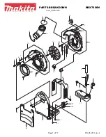
Page 73: ...Maintenance 7B85 Fig 4 9 Cam switch removal procedure 4 1 6 REV AUG 1981 ...

Page 74: ... attach Then disconnect 4 multi pin connectors c Remove the 3 securing screws from circuit board d Lift rear of board and slide toward rear of instrument until board clears the B DELAY MODE switch 3 Remove the TIME DIV and VARIABLE CAL IN knobs as follows a Set the TIME DIV switch to the 2 ms position and the VARIABLE CAL INI knob out to expose set screw b With a hex key wrench loosen the set scre...

Page 75: ...hen the switch is removed the contacts may drop free and be damaged or lost Body salts or acids can contaminate the switch contacts Wear cotton gloves to prevent touching the contacts in the switch or on the board with bare hands Pull the rear of the switch up remove the steel rule and pull the switch out of the front clip To replace the switch first check that the slide contacts are properly inst...

Page 76: ...ylene sheeting to protect the finish of the instrument Maintenance 7885 Fig 4 12 Front panel light socket assembly 3 Cushion the instrument on all sides by tightly packing dunnage or urethane foam between the carton and the in strument allowing three inches on all sides 4 Seal the carton with shipping tape or an industrial stapler __ _____0 1 o _ _ _____ __ 10 30 30 120 120 140 140 160 __ ___ _ __...

Page 77: ......

Page 78: ...erformance of the 7885 every 1000 hours of operation or every six months if used infrequently Before complete adjustment A partial performance check and adjustment may be de thoroughly clean and inspect this instrument as outlined in sirable after replacing components or to touch up the ad Section 4 Maintenance justment of a portion of the instrument To check or adjust only part of the instrument ...

Page 79: ...inimumSp o m Ta e 1 TE T 0W pYN NT Pu o TEKTR0N 70OU s o ProvWooudi oy xun whh orzon d ug n dor ea oompa montn banUwiduh B mp Teat quipmen TEKTRON X7904Ooo ooope TEKTRON X7A10Am d e ug nun a TEKTRUN X7B80TlmoBooo unh b TEKTRON 7B85Tlmo8ooo u TEKTR0N XSG5O4Lovo d SinoVVave 8enamourwi h pow ormodu o U YVavoo 100 Swoap S no G nm u TEKTRON TG501Time K4arkgenera orvvi h po or modu a b TEKTRDN X 9U1Timo...

Page 80: ...Magnified sweep timing check Table 5 1 Cont Purpose Low frequency triggering checks and adjustments Provides access to internal extender adjustments and test points Impedance 50 St type RG Provides signal _ ___ _ 58 U length 42 and 18 interconnections External trigger checks and adjustments Tektronix Part No 011 0049 01 Performance Check and Adjustment 7885 Examples of Applicable Test Equipment a ...

Page 81: ...ep Length and Positioning Range 5 10 horizontal compartment of the mainframe 3 Check Adjust Magnifier Gain and Registration R430 R445 5 11 4 Check Variable Time Division and Variable Hold 4 Set the mainframe vertical mode switch to display the Off 5 11 left vertical unit and the horizontal mode switch to display 5 Adjust Sweep Timing C330 R710 R715 5 11 the A horizontal unit Set the mainframe inte...

Page 82: ...E VARIABLE IN calibrated MAG X1 HOLD OFF MIN A1 Adjust DC Balance and Slope Balance R85 R80 a Connect the low frequency sine wave generator to A2 Check Triggering Modes the amplifier unit input with a 50 S2 cable a Remove the 7885 and plug in extender then install the 7885 directly into the A horizontal compartment b Set the oscilloscope mainframe intensity and focus controls for the desired displ...

Page 83: ...f the waveform j Set the T RIGGERING LEVEL control for a stable dis play TRIG D light on k Set TRIGGERING MODE to SINGLE SWP and the SOURCE to EXT I CHECK Press the SINGLE SWP RESET push button and check that the READY light is on m CHECK for one sweep and that the READY light is out after completion of that sweep when the INT SOURCE push button is pressed oscilloscope intensity may need to be inc...

Page 84: ...al generator to the T connector 1 AC 2 AC LF REJ 3 DC I Set TRIGGERING MODE to AUTO and the SLOPE to i Set the TIME DIV switch to 20 ns Performance Check and Adjustment 7885 n CHECK for a stable display TRIG D light on with the COUPLING switch set to 1 AC 2 AC LF REJ 3 DC Set the LEVEL control as necessary o CHECK_ Set the SLOPE switch to and repeat part n p Set the amplifier unit deflection facto...

Page 85: ...P AUTO and COU s CHECK Set TRIGGERING MODE to P P AUTO and PLING to AC check for a stable display at all settings of the LEVEL con trol TRIG D light on with COUPLING set to h Set the low frequency sine wave generator and the amplifier unit deflection factor for a 2 division display at 50 Hz i CHECK for a stable display TRIG D light on at all settings of the LEVEL control with COUPLING set to j Set...

Page 86: ... TRIGGERING COUPLING to AC and set the d CHECK that the display is not triggered TRIG D LEVEL control for a stable display TRIG D light on light off at either end of the LEVEL control rotation REV AUG 1981 5 9 Performance Check and Adjustment 7B85 A8 Check Line Triggering a Remove all signal connections b Set TRIGGERING SOURCE to LINE the TIME DIV switch to 1 ms and the MAG switch to X1 c CHECK Se...

Page 87: ...nge a Set the mainframe horizontal mode to display the A horizontal compartment Center the display vertically b Horizontally position the display to place the second time marker to the first graticule line a Set the companion time base unit triggering for auto mode ac coupling and internal source Set the companion c CHECK that the end of the sweep extends to at unit for a 1 ms div sweep rate least...

Page 88: ...ter clockwise and check for 2 divisions or less between 5 ms markers c Press in the VARIABLE control for calibrated sweep rates d Set the LEVEL control for a free running display TRIG D light off a Set the TIME DIV switch to 1 ms and set the time e Set the HOLD OFF control fully counterclockwise mark generator for 1 ms markers REV AUG 1981 5 1 1 any slow drift Performance Check and Adjustrnent 7B8...

Page 89: ...s and nines 99 99RE9 on the delay time readout f Check the digital voltmeter readout for 0 100 V within 0 001 V g ADJUST R685 Readout Bias for 0 100 V within 0 001 V h Set the B DELAY MODE switch to B TRIGGERABLE h ADJUST Set the TIME control for the readout nu AFTER DLY merals given in Table 5 2 various symbols will also appear in the readout display and check for the corresponding digital voltme...

Page 90: ...me markers of both delayed sweep traces are horizontally aligned within 0 1 div a Set the DELAY TIME control fully counterclockwise h ADJUST R510 Delay Gain to horizontally align the and set the 0 TIME control for a O time readout of time markers of the delayed sweep traces 8 000 ms i INTERACTIONS Repeat step B until there is no b Set the TIME DIV switch to 2 ms and check for a O change in the adj...

Page 91: ...VM Zero for O time readout of 0 019 ms Then adjust R625 until the O TIME readout just changes to 0 020 ms k Rotate the O TIME control fully counterclockwise B10 Adjust DVM Gain 8620 a Set the DELAY IME control to start the first intensi fied zone on the second time marker and set the TIME control to start the second intensified zone on the tenth time marker Further rotate the D TIME control to hor...

Page 92: ... divisions below graticule center horizontal compartment Then install the 7885 directly into the A horizontal compartment b Set the TRACE SEP control to position the second delayed sweep trace approximately 0 2 div below the first delayed sweep trace a Set the 7885 TIME DIV switch to 10 us and set the companion time base unit for a 0 2 s div sweep rate c Set the time mark generator for 0 2 s marke...

Page 93: ...of 1000 ns 0 1 ns ___ 1 s _ 4 0 ns h 0 3 ns i 0 1 ns __ 4 4 ns 2 s Therefore the specified limits for a measurement in 5 s terval of 800 ns are 800 ns 4 4 ns 795 6 ns to 804 4 ns h CHECK Follow the procedure outlined in parts c through g and check for TIME accuracy as given in Table 5 3 5 S___ _ ____ _ 5_ S___ _ _ __ _5_ S _ _ _ 39 77 s to 40 23 s 1 s 10 ws 79 56 s to 80 44 ws s _ _ __ 20 us _ 1 5...

Page 94: ...t to Delaying Sweep Display c Position the delaying and delayed sweep traces to start on the first graticule line B17 Check Delay 7irr e Jitter a Set the companion time base unit sweep rate to 2 us div Set the time mark generator for 10 s markers b Set the DELAY TIME control for a delay time readout of approximately 1 000 ms a Set the TRACE SEP control into the OFF detent to c Set the DELAY TIME c...

Page 95: ...nter 8 divisions within the tolerance given in 1 able 5 4 Set the POSITION controls and TRIGGERING LEVEL control as necessary for a stable display aligned with the vertical graticule lines NOTE If the time mark generator used does not have 1 2 5 sequence markers apply unit markers in place of 2 unit markers and check for 2 markers div over the center 8 divisions of display to the tolerances given ...

Page 96: ...ns Within 0 32 div _ _ ___ _ __ ___ l_______ ___ ____ __ _____ ___ _ ________ ______ _ ________ 50 ns 5 ns Within 0 32 div 1 s 10 ns Within 0 2 div 2 s 20 ns Within 0 2 div 5 s 50 ns Within 0 2 div 1 s 1 s Within 0 2 div _______ _ ____ _ _ ___ _ __ ___ _ _e _____ _ _ __ _ ___ _ __________ _ _ This completes the Performance Check and Adjustment 2 s 2 s Within 0 2 div procedure _ _____ _ 5 s ___ 5 s...

Page 97: ......

Page 98: ...6 7885 No options were available for this instrument at the time of this printing Information on any subsequent options may be found in the CHANGE INFORMATION section in the back of this manual REV AUG 1981 6 1 ...

Page 99: ......

Page 100: ...ct you concerning any change in part number Change information if any is located at the rear of this manual SPECIAL NOTES AND SYMBOLS X000 Part first added at this serial number OOX Part removed after this serial number ITEM NAME In the Parts List an Item Name is separated from the description by a colon Because of space limitations an Item Name may sometimes appear as incomplete For further Item ...

Page 101: ...RIEL CA 91776 17856 SILICONIX INC 2201 LAURELWOOD DRIVE SANTA CLARA CA 95054 18324 SIGNE TICS CORP 811 E ARGUES SUNNYVALE CA 94086 24546 CORNING GLASS WORKS ELECTRONIC COMPONENTS DIVISION 550 HIGH STREET BRADFORD PA 16701 27014 NATIONAL SEMICONDUCTOR CORP 2900 SEMICONDUCTOR DR SANTA CLARA CA 95051 32293 INTERSIL INC 10900 N TANTAU AVE CUPERT INO CA 95014 32997 BOURNS INC TRIMPOT PRODUCTS DIV 1200 ...

Page 102: ...0820K C51 283 0111 00 CAP FXD CER D1 0 1UF 20 50V 72982 8121 N088ZSU104M C52 283 0111 00 CAP FXD CER DI 0 1UF 20 50V 72982 8121 NOSSZSU104M C53 281 0773 00 CAP FXD CER DI 0 01UF 10 100V 04222 SA201C103KAA C56 283 0010 00 B010100 8039999 CAP FXD CER DI O OSUF 100 20 50V 56289 273C20 C56 283 0341 00 B040000 CAP FXD CER DI 0 047UF 10 100V 72982 8121N153X7R0473K C57 283 0203 00 CAP FXD CER DI 0 47UF 2...

Page 103: ...L C526 290 0527 00 CAP FXD ELC1Lf 15UF 20 20V 90201 TDC156M020FL C530 283 0111 00 CAP FXD CER DI 0 1UF 20 50V 72982 8121 N088Z5U104M C532 283 0111 00 CAP FXO CER DI 0 1UF 20 o 50V 72982 8121 NOSSZ5U104M C556 281 0826 00 8092075 CAP FXD CER DI 2200PF 5 100V 12969 CG8222KEX C573 290 0527 00 CAP FXD ELCTLT I5UF 20 20V 90201 TDC156M020FL C576 283 0111 00 8050000 8088749 CAP FXD CER D1 0 1UF 20 50V 729...

Page 104: ...8 152 0141 02 SEMICOND DEVICE SILICON 30V 150MA 01295 1N4152R CR250 152 0141 02 SEMICOND DEVICE SILICON 30V 150MA 01295 1N4152R CR252 152 0141 02 SEMICOND DEVICE SILICON 30V 150MA 01295 1N4152R CR254 152 0141 02 SEMiCOND DEVICE SILICON 30V 150MA 01295 1N4152R CR255 152 0141 02 SEMICOND DEVICE SILICON 30V 150MA 01295 1N4152R CR256 152 0141 02 SEMICOND DEVICE SILICON 30V 150MA 01295 1N4152R CR264 15...

Page 105: ...150MA 01295 1N4152R CR752 152 0141 02 SEMICOND DEVICE SILICON 30V 150MA 01295 1N4152R CR753 152 0141 02 SEMICOND DEVICE SILICON 30V 150MA 01295 1N4152R CR754 152 0141 02 SEMICOND DEVICE SILICON 30V 150MA 01295 1N4152R CR763 152 0141 02 SEMICOND DEVICE SILICON 30V 150MA 01295 1N4152R CR772 152 0141 02 SEMICOND DEVICE SILICON 30V 150MA 01295 1N4152R CR773 152 0141 02 SEMICOND DEVICE SILICON 30V 150M...

Page 106: ...N NPN 04713 SPS8026 0264 151 0223 00 TRANSISTOR SILICON NPN 04713 SPS8026 0272 151 0223 00 TRANSISTOR SILICON NPN 04713 SPS8026 0274 151 0223 00 TRANSISTOR SILICON NPN 04713 SPS8026 0282 151 0190 00 TRANSISTOR SILICON NPN 07263 5032677 0284 151 0223 00 TRANSISTOR SILICON NPN 04713 SPS8026 0288 151 0190 00 TRANSISTOR SILICON NPN 07263 S032677 0292 151 0190 00 B010100 8088749 TRANSISTOR SILICON NPN ...

Page 107: ...CON NPN SEL FROM MPS652 04713 SPS8801 0618 151 0410 00 8010100 8088749 TRANSISTOR SILICON PNP 80009 151 0410 00 0618 151 0216 00 B088750 TRANSISTOR SILICON PNP 04713 SPS8803 0632 151 0192 00 B010100 8088794 TRANSISTOR SILICON NPN SEL FROM MPS652 04713 SPS8801 0636 151 0220 00 8010100 8088794 TRANSISTOR SILICON PNP 07263 S036228 0642 151 0192 00 8010100 8088794 TRANSISTOR SILICON NPN SEL FROM MPS65...

Page 108: ... 25W 01121 CB6225 R55 315 0202 00 RES FXD CMPSN 2K OHM 5I 0 25W 01121 CB2025 R56 315 0104 00 RES FXD CMPSN 100K OHMS 0 25W 01121 CB1045 R57 315 0104 00 RES FXD CMPSN 100K OHM 5 0 25W 01121 C81045 R58 321 0443 00 RES FXD FILM 402K OHM 1 0 125W 91637 MFF1816G40202F R59 321 0443 00 RES FXD FILM 402K OHM 1 0 125W 91637 MFF1816G40202F R60 311 1192 00 RES VAR NONWIR IOK OHM 20 1 W W SW 71590 BA 232 001 ...

Page 109: ...637 MFF1816G97600F R217 321 0291 00 8030000 RES FXD FILM IO SK OHM 1 0 125W 91637 MFF1816G10501F R218 321 0274 00 8010100 8029999 RES FXD FILM 6 98K OHM 1 0 125W 91637 MFF7816G69800F R218 321 0267 00 8030000 RES FXD FILM 5 9KOHM II 0 125W 91637 MFF1816G59000F R222 315 0472 00 RES FXD CMPSN 4 7K OHMS 0 25W 01121 CB4725 R224 315 0622 00 RES FXD CMPSN 6 2K OHM 5 0 25W 01121 CB6225 R226 315 0393 00 RE...

Page 110: ...ES FXD CMPSN 220 OHM 5 0 25W 01121 CB2215 R303 315 0470 00 RES FXD CMPSN 47 OHMS 0 25W 01121 CB4705 R304 315 0103 00 RES FXD CIt4PSN 10K OHM 5 0 25W 01121 CB1035 R305 311 1228 00 RES VAR NONWIR IOK OHM 20 O SOW 32997 3386F T04 103 R307 321 0301 00 RES FXD FILM 13 3K OHM 1 0 125W 91637 MFF1816G13301F R308 321 0275 00 RES FXD FILM 7 15K OHM 1 0 125W 91637 MFF1816G71500F R312 315 0201 00 RES FXD CMPS...

Page 111: ...D CMPSN 68 OHM 5 0 25W 01121 086805 R424 323 0285 00 RES FXD FILM 9 09K OHM 1 0 50W 75042 CEGTO 9091F R426 315 0180 00 RES FXD CMPSN 18 OHM 5 0 25W 01121 081805 R427 315 0103 00 RES FXD CMPSN IOKOHM 5 0 25W 01121 081035 R428 315 0473 00 RES FXD CMPSN 47K OHMS 0 25W 01121 CB4735 R430 311 1423 00 RES VAR NONWIR 20 OHM 20 0 50W 73138 72 1 0 R431 321 0122 00 RES FXD FILM 182 OHM 1 0 125W 91637 MFF1816...

Page 112: ...R536 321 0342 00 8010100 8088749 RES FXD FILM 35 7K OHM 1 0 125W 91637 MFF1816G35701F R536 321 0340 00 8088750 RES FXD FILM 34K OHM 1 0 125W 91637 MFF1816G34001F R537 315 0511 00 RES FXD GMPSN 510 OHM 5 0 25W 01121 CB5115 R541 321 0097 00 8010100 B088749 RES FXD FILM 100 OHM 1 0 125W 91637 MFF1816G100ROF R541 315 0101 00 8088750 RES FXD CMPSN 100 OHM 5 0 25W 01121 CB1015 R542 315 0154 00 RES FXD C...

Page 113: ...25 R628 321 0257 09 BO10100 8088749 RES FXD FILM 4 64K OHM 1 0 125W 91637 MFF1816C46400F R629 321 0257 09 8010100 8088749 RES FXD FILM 4 64K OHM 1 0 125W 91637 MFF1816C46400F R631 321 0289 06 B088750 RES FXD FILM IOK OHM 0 25 0 125W 91637 MFF1816C10001C R632 315 0432 00 B010100 B088749 RES FXD CMPSN 4 3K OHM 5 0 25W 01121 CB4325 R632 321 0289 06 8088750 RES FXD FILMaOK OHM 0 25 0 125W 91637 MFF181...

Page 114: ...B010100 8088749 RES FXD CMPSN IK OHMS 0 25W 01121 CB1025 R699 315 0273 00 8010100 8088749 RES FXD CMPSN 27K OHM 5 0 25W 01121 CB2735 R705 311 0467 00 RES VAR NONWIR 100K OHM 20 0 50W 11237 300SF 41334 R706 321 0438 00 RES FXD FILM 357K OHM 1 0 125W 91637 MFF1816G35702F R710 311 1232 00 RES VAR NONWIR 50K OHM 20 0 50W 32997 3386F T04 503 R711 321 0458 00 RES FXD FILM 576K OHM 1 0 125W 91637 MFF1816...

Page 115: ...ro 0 25W 01121 C85105 R832 315 0150 00 RES FXD CMPSN 150HM 5 0 25W 01121 C81505 R841 321 0260 00 RES FXD FILM 4 99K OHM 1 0 125W 91637 MFF1816G49900F R842 321 0289 00 RES FXD FILM IOK OHM 1 0 125W 91637 MFF1816G10001F R844 315 0101 00 RES FXD CMPSN 100 OHM 5 0 25W 01121 CB1015 S10 263 0010 01 SWITCH PB ASSY 1 PUSH 7 5 MM 1 CONTACT 80009 263 0010 01 S20 263 0016 00 SWITCH PB ASSY 4 LATCHING 7 5 MM ...

Page 116: ...RCUIT DI QUAD 2 INP NAND GATE 80009 156 0113 00 0662 156 0030 00 8088750 8091399 MICROCIRCUIT DI QUAD 2 INPUT NAND GATE 01295 SN7400 N OR J U662 156 0030 03 B091400 MICROCIRCUIT DI QUAD 2 INPUT NAND GATE 27014 DM8000 U682 156 0041 00 MICROCIRCUIT DI DUAL D 1YPE FLIP FLOP 27014 DM7474N 0686 155 0090 00 B010100 8059999 MICROCIRCUIT DI MONOLITHIC 4 DECADE COUNTER 80009 155 0090 00 0686 155 0171 OD 80...

Page 117: ......

Page 118: ...ies on the diagrams A Assembly separable or repairable H Heat dissipating device heat sink S Switch or contactor circuit board etc heat radiator etc T Transformer AT Attenuator fixed or variable HR Heater TC Thermocouple B Motor HY Hybrid circuit TP Test point BT Battery J Connector stationary portion U Assembly inseparable or non repairable C Capacitor fixed or variable K Relay integrated circuit...

Page 119: ...CATIONS B C SIGNAL DIODE __ mI PLASTIC CASE _ J TRANSISTORS INDEX 5 A LIGHT EMITTING DIODE L E D TRANSISTORS 14 G INDEX PLASTIC CASE rv DUAL ME7 AL FETS CASE FET INDEX INDEX INTEGRATED CIRCUITS 1 v I G I I I GJ IdS D SINGLE B METAL CASE Fig 8 1 Semiconductor lead configurations REV JUL 1981 E 1986 66 1961 72 ...

Page 120: ...Fig 8 2 Location of circuit boards in the 7885 ...

Page 121: ...nwcn R427 CR423 x428 Q424 R445 5435 R44J 8446 8444 _ C448 0441 R424 R448 _ 0440 R440 o e R448 R4 7 f R456 R432 8 R4 3 Q438 Q434 R430 CR433 w o _ _ Fig 8 5 A3 Readout circuit board assembly 53 R353 Y8114 iZll_ 0124 8717 8115 CS71E A314 8329 CR31a B323_ gam 8321 _ 813 5 R325 R322 C312 CR334 L11 m 8335 Q324 p322 VRZ28 334 C334 k CR3 4 CR12 3 See Parts List for serial number ranges Fig 8 3 A7 Interfac...

Page 122: ...2 _ 4 R509 C62y R513 d 64A _ _ 8510 CR643 U 608 H _ R621 1 85e4j R644 by e 9582P B592 v CR249 R555 A2 TRIGGER A53q 9 z s P 3H t N7R5F C255 CR264 _ CR292 CR296 CR252 CR293 CRZl4 0 252 r m A 25i CR288 t8292_i e a yn2en A293 R654 _r gz5a uzso cfl 9fLi9 _ R683 y t Rs76 g263 CI264 WY612 C 263 x CR259 J 500 CR291 Fig 8 6A A4 ISN 8088750 Up Digital Voltmeter circuit board assembly REV JUL 1982 a 15e_S_ o...

Page 123: ...654 uaa _ tCp25x R292 P 95 R R662 i R25fi 8255 CR288 R8 2 9 1 4 r R290 R6i5 i R661_I C699 Rfi71 R250 Rfi78 8699 8 6 74 i R251 R293 Q676 Rf fi73 CR2 4 r V U250 CR286 a R679 RL r2 P 64 R297 C679 _ IR262 CR255 r 8676 R61 n R286 T 8284 gq j R291 CR258 tt _ 263 _ CR291 l_c R92 R4 8 Q48 R49 Fig 8 6B A4 SN B088749 Below Digital Voltmeter circuit board assembly R537 C520 RL _531 __ n R533 R515 3 R532 _ 65...

Page 124: ... F F_ _ _ _ EFF SN 60 8 f49 a ovY CROM GR543 R541 01 R254 P295 R295 13 A4 R294 I SEPARATIO I5V 15V CI o OfF I sV wVV K54T U53D8 5 f I U530A 3 iI51 PARTIAL A4 DV M 130AR _ lu P530 R520 DELAY TIME R53D TIM6 5205 B DELAY MODE 7885 qG a LEVEL v o qv N04 SnNf a iNOs d 5 AFT Q531 fir 3 I y TRI AGTF ...

Page 125: ... 1 21 15Y x515 USD08 5 f I4 I 8551 3 YI V6304 i I S I 1961 60 REV JUL 1982 8295 7RALC SG R510 DELAY TIME o4RTIAL AZ TRIGGER 3OARD iROM To GRT14 CRT23 CRT75 RT25 530 CGAL15 VARWOLE TIME Static Sensitive Devices See Mamfenance Secfron PARTIAL A4 DYM lOARD PARTIAL A3 REP 0OVT 3Q4RD v41D ISV RH2 I I4I R410 U41lo 2 Po5ITION R1 41 I I3I R4I5 L yy FIN i _ 15V iJl I PTOS 50V RT05 R706 I3I 3wP r r II D2 0 ...

Page 126: ...3 5D J500 5J CR301 2E L274 5A CR302 2F L326 3G CR314 2G L382 58 CR323 3G LR326 3G CR324 3G LR810 3B C8334 2F LR820 3B CR344 1B LR830 3B 8451 8456 CR526 0562 _R526 C526 0512 R518 CR356 8514 0516 x 51 p3521 p 56 835 564 C522 522 8305 4 VR314 8524 8354 C324 0522 8521 0528 _ _ 8303 8315 56B R52B 8308 TY p3 8 p3d s 8314 _ 8422 fl3 i1 345 0304 G P 8323 8434 8301 R439 CR301 fCR3D2 8313 8321 8339 8325 Fig...

Page 127: ...20 Pg10 ooo _ OB44 fl243 _ J300 0225 _R2_4_q _ CR224 R240 R224 m R242 R99 m C99 0242 0204 R204 C221 _ R207 v 241 R356 CR208 Cg2pB R20B R206 C356 R231 0358 0206 023D 0234 R3_56 _ 8203 a C204 L2 R 02 R 0202 0201 C1I3 f F R2_1I r R 3 CR 1 0362 A203 8234 mil e R205 a R448 3D R575 4D R749 4F R449 3C R576 4D Rg21 5C R454 3C R577 5C R832 1J R455 3D R578 4B R841 2J R456 3D R706 1H R842 2J R457 3C R710 1F ...

Page 128: ...4 2p P60 3B R32 5C R57 3C R93 1D C20 5A C85 2D R33 5C R58 3C R94 1D C21 5B C88 1E 022 4B R34 5C R59 3C R95 1D C22 5B C89 2E 048 2E R35 4C R61 2C R96 2E C23 4B C92 2E 088 2D R36 4C R62 1C R97 1D C30 4A 092 2D R37 4C R63 1C R98 2E C34 5C CR23 4B 096 1D R3g t qg R64 3B C35 4C CR24 4B 098 1E R41 4B R65 3B S10 4B C37 4B CR53 28 R42 4A R67 5B S20 1B C43 2C CR55 3A R8 3A R43 3C R68 3A S50 1B C46 3C CR71 ...

Page 129: ... SEP fully counterclockwise Voltage Conditions The voltages shown on the diagram were obtained using a digital multimeter with a 10 MS2 input impedance Tektronix DM 501 Digital Multimeter or Tektronix 7D13 Digital Multimeter used with readout equipped 7000 series oscilloscope Waveform Conditions The waveforms shown below were obtained using a test oscilloscope system with 10 MS2 input impedance an...

Page 130: ... C4I RGI 6I 6 9Bk C51 ay9 0 1 B1 R d1 LnG3 1 a k5 Gasc 1 G5 I iok ol Q46 U55A sa 5k 0 8 i STaI 1y SOURCE INT F L elc FLRTIAL __ 900 I PEAK C PEAK AUTO 3 I IgyG V o l 8 Cob 5V T L 0 c 5u0 P EJECT S CZ3 AND 001 OWSINy CtW TRI4CTER 50 JRGEI BE A1 p D O gUT0 4M G R50 Jzls L S N T3 s isk L50 Gpn I G u sa Rsb R1M L011 r1T1i 5 ISV b OOk y CRlS 8 _ T b GI RT R U556 a a s ooik cT5 k1Tal 15V 01 asT opk CsT ...

Page 131: ...L 510 COUPLING AC NF EJ T 5 Y aB4t1C80 SY re6fT pI 45V SLOPE BAL 5V a80 tpk TRIG G ER C N RA OR C r FROM _ i u z c j D O z static Sensitive Devices Pbp s J oo 4 5 eeMamlenance SecOan anVUECw TH_ _ SLOPE QVEL ARIS SvrEw START GATE GATE C PARTIAL AI INTERLACE DD I ti i2_B Q322 D 4 TRIGGER GENERATOR IREARINTERFACE 5 10 CONNECTION ...

Page 132: ...CR634 R592 p 582 C627 CR24B S 205 R625 R544 _ r r R254 D 592 R622 p 288 8687 R547 0687 R620 R281 R282 D 546 U 556 U 53 0 53fi R531 C529 R531 a z Q R535 R533 U R515 R531 C532 p 548 p 282 CR250 R548 8253 CR543 R631 CR548 8288 9 p 2 P 38 H285 a C 255 CR254 CR292 C694 0691 0692 c CR252 CR293 R636 D 252 8292 m R R653 R255 CR288 i 1 U662 U666 R681 I R6R2 R248 R250 C693 R264 Q 0293 C686 Rfi54 R678 R672 R...

Page 133: ...ection REV JUL 1982 C255 4E CR264 4F C263 5F CR286 4G C520 2G CR28B 4F C530 1G CR291 SG C532 2G CR292 4F C608 2D CR293 4F C627 3D CR294 4G C645 4C CR295 4G C652 3D CR296 4G C654 4C CR543 3B C662 4C CR627 1E C676 5E CR641 2D C679 5E CR642 2D C683 58 CR683 58 C684 4B CR6B4 48 C6B6 48 C691 3B J100 1D C692 4B J500 5E C695 4B C697 3B L691 4A C699 4D L692 48 L697 4A CR248 2F CR250 3F P31 3D CR252 4F P32...

Page 134: ...3 2G R534 2G R535 2F R536 2F R537 1G R541 3C R544 3F R545 3F R546 2F R547 3F R548 3E R549 3D R552 tE R554 2F R555 2F R582 2F R592 2F R605 1C R606 lE R607 1E CB627 R616 y R52 y R554 e _ R509 GRID COORD CKT NO R613 2E R614 3E R615 2D R616 1F R617 1F R618 1E R620 3D R621 3D R623 1D R624 2D R625 1C R626 2D R627 2D R628 1F R629 2F R632 2E R634 3C R635 2C R641 2D R642 2D R645 4C R646 5C R653 3C R654 4C ...

Page 135: ...re obtained using a digital multimeter with a 10 MSZ input impedance Tektronix DM 501 Digital Multimeter or Tektronix 7D13 Digital Multimeter used with readout equipped 7000 series oscilloscope Waveform Conditions The waveforms shown below were obtained using a test oscilloscope system with 10 MS2 input impedance and at least 60 MHz bandwidth Tektronix 7603 Oscilloscope 7B53A Time Base and 7A13 Di...

Page 136: ...CONTROL READY 11 uyNT 9 tiIOLD OFF 6V SV RC slyk 42D4 C11I 7T 100 I SWP pISABLEL OUT 16 HOLD OFF START SINGLE SWEED RESET LOyIC 615 4153 5V a2ns a7o R207 gzoz 619 OR208 cRxD1 LOGKpUT a2o SY ___ __ To e R10f1 I q R20I p Z 5T5 11S 3 9k OELAY GATE 4203 NCKWT 2lk I I JSOD i7v 110 Z I I I Hoio osc r N YC H 8103 W I 390 15 sv Q201 E p TIME ENABLE Rv 6204 FROM CR148 16Y ool 9 s 454ro c O Rs sY _SY 1 1 2K...

Page 137: ...R292 I 1 5k 8191 2k SV 5V R264 J500 C263 R163 Ik CR2b4 f3l j 3 t 1k H Q264 8161 a 1K Q262 Q292 p195LY Y Y 8195 Sk TRACE SEP Q254 PARTAL 5205 DELAY MODE INDEPENDENT U 250 D y1141I1 0 153 4254 R254 7 Ca291 SZCR193 R25k Q294 R293 CR195 I C R196 30k CR29 16Y j jR286 R196 8194 56k 4 3K 4 3K I5V _ __ _ aAM4ED WITH 5195 5 sv s1 r o Q234 15Y I IOLDOFF OUTPUT 8111 AM PL 4 Tk ca1 3 __ sv 6515 ISY 01 Q212 42...

Page 138: ... CR753 2B R754 28 R785 2A CR754 2B R755 2C R786 2A CR763 2F R756 2C R787 2C CR772 2D R757 2C R791 2E CR773 2D R761 2F R792 2E CR782 2D R762 2F R793 2E CR783 20 R763 2H R794 2E CR785 2A R764 2F CR786 2A R771 2D 5725 2C R772 2D S800 1C P21 1H R773 2D R779 2D R725 2H R781 2D Fig 8 10 A3 Readout circuit board assembly Static Sensitive Devices See Maintenance Section REV 1UL 1981 A1 INTERFACE A B C _ _...

Page 139: ...1961 55 ...

Page 140: ...s shown on the diagram were obtained using a digital multimeter with a 10 MS2 input impedance Tektronix DM 501 Digital Multimeter or Tektronix 7D13 Digital Multimeter used with readout equipped 7000 series oscilloscope Waveform Conditions The waveforms shown below were obtained using a test oscilloscope system with 10 MS2 input impedance and at least 60 MHz bandwidth Tektronix 7603 Oscilloscope 7B...

Page 141: ...132 look 8 TOV R124 R722 R723 b sk z15k io3k PARTIAL AI INT A jPAarInLA3READOUT aD AXIS GA I FROM J1D0 G 51258 _______SEfiDVA jO ITIMINCs CURRENT 29 PARTIAL _ SOURCE M cR723 c lia 28L nneE Dw 4 __ _ __ 1lll 4 I2 R741 5 SR741 8743 8744 8745 R746 Rl4l RT48 R749 516 c 27k 4 000NS S1 b61M i broM BOOk 1661k Ib0 0k 80 00k 2b bik Ib OOk GR3240 330 6331 R33b Z I p T11 PnannL loo Q338 SOxS r I TIME DIY Tv3...

Page 142: ...UT 6156 5V 0 7 8258 Q3b2 G 3b2 Q3 2 2k R38i b 8747 RT48 8749 FROM Qua R3 15V Ok 80 k 2b 67K 16 OOk CR10a OtAyO R 56 2S7k v5v NOLDOFF STAR TO V 21 O I e REFEREN E R3a3 5 36k To ilo0 I O 8344 t5V GR34 0 30 8341 0 7 I R3ab l I d 99y o ov Q344 a 7k 1R7 a7 A3 A SWEEP 83 8 SWEEP iok Q34 o t ISv w R402K 8470 1507 _15V R3as OuTPUT 2 4k 5Y 5y PREAMPLI F IER R4a9 2 tOk w4 All SIyNAL Q448 ae 4428 aiK 9 CR423...

Page 143: ...own on the diagram were obtained using a digital multimeter with a 10 MS2 input impedance Tektronix DM 501 Digital Multimeter or Tektronix 7D13 Digital Multimeter used with readout equipped 7000 series oscilloscopel Waveform Conditions The waveforms shown below were obtained using a test oscilloscope system with 10 MS2 input impedance and at least 60 MHz bandwidth Tektronix 7603 Oscilloscope 7B53A...

Page 144: ...orn 2 6Y I _ R e1D DIAC e oo c Ay 4 OT O tiMa O RS W TIME h49LE 20W5 51 i r a a __ __ Roh AcoID iooklr _ UbSb b Dl y R52j 00 ae cwy e asaa 4582 20Ck Q546 R545 43k yv r SV RSa gaRT14L 5105 2 w Q548 a EUY uwDE INDEPENDENT T 5EE DIAy GRSa3 READC T DATA ROM 01 C _ GCLUMN FPN LCGE 752 A93 _ yw o 839 A a RaM Ps4i ACa P DfAV O SOk L0 s pt r NTE4cA E 3 o v12 P1 I H i OLLIMN I y yy i E aSx 4ALDV 3DG t D474...

Page 145: ... S _ tGOMPARaTOR I DELAY GATE i GENERATOR c556 2200 P295 L Y v295 Lsl3 TS2 A33 E Static Sensitive Devices See Mamlenarlce SeUion FISV r15Y asla R52b 4 99k 0 99k Q ia GR52b rIS IV 1C51b R517 16 yF 9 09k 8514 11D ISV i Isv ISV 5295 TRACE SEP pFFd INf GArv ED WITH 4295 f ____ RSbb 51k C579 I Y 4TH R56D 32 Lo7p Q5 o2 5k Q568 czsb7 R561 I 13 IL _ISY ISV 24k QSw4 Rsb S iak Lbk 8591 Q 92 COMPAFISON ISV 1...

Page 146: ...s The voltages shown on the diagram were obtained using a digital multimeter with a 1 M O input impedance Tektronix DM 501 Digital Multimeter or Tektronix 7D13 Digital Multimeter used with readout equipped series osci Iloscope Waveform Conditions The waveforms shown below were obtained using a test oscilloscope system with 1 Mfg input impedance and at least 15 MHz bandwidth Tektronix 7603 Oscillos...

Page 147: ...Pp CONVERTER OELAY COMPARISON 55k L1 30 voLTA e2 CR643 Q o44 FROM Q5a2 4592 6 ROOk Gw Rb22 R e23 1 X716 35 549k f15V R1o26 fs OVM CTAIN Rlo25 SIk R64 SOY _________ J 12 __ b1z sov 2 I I ___ ____ b H l OOONC SAN OOO f1c 1cv 000NN V _ n _ n 1 P32 N TIME DIV PART IAL 5800 SHOWN ItHS POS N SOV Rbn a a7k 8031 U55 o8 36 1458 1 Io ok Rro3i r 5 CR63t 1_1k 3 R n31 GR635 56 lO Ok 15V 20k G4 R e14 V a LB DVM...

Page 148: ... R67b y 47 k II Se EL k 8 VRbg4 R044 bzv 1 9p 5 I C0ADTER MEMORY 191 68 REV JULY 1981 RwBI 2k R o 2 i 3k 39 I3 GT C b9lo 050 r COUNTER E N000ER is Rr 6 5 a 3 R i Rs Z RS j Rsa VEE ISV r pIGKOFF REFERENCE To 453 8 iJ Rb83 33 0 9 ASV CURRENT 19 OUT READOUT DATA ro 5205 Static Sensitive Devices See Maintenance 5ec6on IREARINTERFACE CONNECTION PARTIAL A4 DVM BO sN aos875o uF DICaITAL VOLTMETER DVM ...

Page 149: ...erclockwise Voltage Conditions The voltages shown on the diagram were obtained using a digital multimeter with a 10 MS2 input impedance Tektronix DM 501 Digital Multimeter or Tektronix 7D13 Digital Multimeter used with readout equipped 7000 series oscilloscope Waveform Conditions The waveforms shown below were obtained using a test oscilloscope system with 10 MSZ input impedance and at least 60 MH...

Page 150: ... 3 32k 3130 3 I e 4 oboe 270 15V R614 v53 Q612 2 k 4 64 k 5v 8634 5V 2k C65 15V 8629 R635 5V b g 4 64k 63k Q632 3 9k Q652 u65 U5568 7 Yz sssa 5 a R62e cbsz 3300 Rb 5V 241 OELAV DVM CCMDARISCN GAIN R611 0626 voLTAGE O az ok 1 7aysv 4y FROM 1582 E 8592 R620 b 5k ooov n 3 d R627 _ gy 1 5 k 15V 8616 8623 IOOk 43k R625 20 k R615 1 3k 15V 33 k 5v U698A 15V Rb9g 5V Ik y2 7474 5V SR646 5 R 5 5V 3 3k p 3 C...

Page 151: ...4 S 2 COUNTER 4ND MEMORY P32C e X T T T 8654 C654 18k U662C 036 45 p I a 7aoo 15Y 5V a B R681 I4 13 12 II 5 1 k 5V 4Y r57 T5 r5 5 rsa I 5V AIR A e 6 T54 Tp O SNBOEe749 gE Low DIGITAL VOLTMETEfL DVM U686 SWP CAL VOLTACsE REFEREN E TO q53 B READOUT DATA TO 5205 y SV I TYPE Vcc fiND 74001 14 1 79 14 14 1 5V Static Sensitive Devices R672 c676 13 k R682 U682A See Maintenance Section a55 5V Ik vs 7a7a 2...

Page 152: ...I I UNCAL O o I I I I I PI 021 i 1 I I I I 1 I I I TS 3 831E fir I i i v li 1 I I I I I I 1 1 1 0I 161 1 I 1 I I I I I Ts I B33 r54 1 e gel 112 5 I I I I I _ I I I 1 I FROM OT7 I I 1 I I I I T58 A30 n 1 lo l l91 I I 1 i 1 I I I 1 I I I I T s 9 029 1 e 1 I I I I I I 1 I I I 1 I I I I I I I TS 1 To I I I I I 1 x435 I I I I I I I 1 I I I I I I I I I 1 I I I I I I 1 1 1 I 1 I I I I 1 I I 1 I I I I I I...

Page 153: ... 1 i PARTIAL A3 REAbOUT flOARp I PARTIAL AI INTERFACE pARD See Maintenance Section TIME DIVISION AND READOUT SWITCHING Q TIME DIV 0 INDICATES SWITCH CLOSED tatlC Sensitive DCVIC2S jREAR INTERFACE W N I N I Nt t S DOS CONNECTION ...

Page 154: ...3o F Ts To I 29 i 28 i 27 I 26 I I 13 aND TD C NO I SINGLE SWEEP I FRph 1AR234 READY INDICATOR t0 sv uyHTS s F I LINE TRICaC ER 4 TO R29 2O I A SWEEP 3 2 I SW EEP GATE I FROM R3g3 I 24 30 sv 23 I LR820 rFi2rG I 200 H R821 51 iSV 22 I oi Dc PL To T35 I 1 ao 5ov colo I i I S V I i I 16 SINGLE SWEEP I CROM U220 f LOyIG 15 I FROM R341 FROM W 4 TRIyyERINC DSSID 6 DELAY MOOE PB20 D 0 j ISV f E SV 5V DAR...

Page 155: ...N MODE 34 33 T5 32 T5 TO C j 31 TS 30 T5 29 TSB 28 25 24 j 29 22 0 2I To T35 _ 20 rRly IN i5Y o n IB tSVPOWEI v3 I 30 E 11 P8 4 I o AUX Y AX15 5230 f 15 SINGLE SWEEP RESET F9 3 14 DUAL SEAM AUK Y AXIS 13 12 CaN D I I SIGNAL 10 X Y COMPENSATION 9 CELAY GATE Q20 f 8 SWEEP LOGkOUT I MAJN FRAME FB_2 l CHANNEL SIntTLH I SIGNAL 6 5 R2T5 4 HOLD OFF 3 SWEEP J500 I 2 OUT DELAY MODE 0220 I3 j I tN CONTRDL 1...

Page 156: ...A2 TRIGGER A1 INTERFACE R80 SLOPE BAL Fig 8 12 Location of Triggering adjustments ...

Page 157: ...B088750 Upl Location of Digital Voltmeter adjustments R445 R710 R715 MAG REG 10 us TIMING 10 ms TIMING R430 I C330 MAG GAIN R305 50 ns TIMING 1961 74 DELAY START R535 PICKOFF BIAS R555 DELAY OFFSET Fig 8 11 Location of Sweep Timing adjustments P3 TESTI CONNE P TEST CONNE ...

Page 158: ...715 TIMING J MING ning adjustments 1961 67 R685 READOUT BIAS R620 DVM GAIN 1961 59 Fig 8 138 SN B088749 Below Location of Digital Voltmeter adjustments R535 SECOND PICKOFF BIAS R555 DELAY OFFSET ...

Page 159: ......

Page 160: ...ure and index numbers to the illustrations In the Parts List an Item Name is separated from the description by a colon Because of space limitations an Iterel Name may sometimes appear as incomplete For further Item Name identification the U S Federal Cataloging Handbook H6 1 can be utilized where possible A VIA T I N ITEM NAME INCH ELC7HN ELECTRON IN INCH SE SINGLE END NUMBER SIZE ELEC ELECTRICAL ...

Page 161: ...INTOWN PA 19046 57668 R OHM CORP 16931 MILLIKEN AVE IRVINE CA 92713 71159 BRISTOL SOCKE7 SCREW DIV OF AMERICAN CHAIN AND CABLE CO INC P O BOX 2244 40 BRISTOL ST WATERBURY CT 06720 71590 CENTRALAB ELECTRONICS DIV OF GLOBE UNION INC P O BOX 858 FORT DODGE IA 50501 71785 TRW CINCH CONNECTORS 1501 MORSE AVENUE ELK GROVE VILLAGE IL 60007 73743 FISCHER SPECIAL MFG CO 446 MORGAN ST CINCINNATI OH 45206 73...

Page 162: ...105 0076 04 18 214 1280 00 1 SPRING HLCPS 0 14 OD X 1 126 L 0 16 DIA 80009 214 1280 00 19 333 1836 00 8010100 8085809 1 PANEL FRONT 80009 333 1836 00 333 1836 01 B085810 1 PANEL FRONT 80009 333 1836 01 20 378 0074 00 14 REFLECTOR LIGHT PUSH BUTTON 80009 378 0074 00 21 366 1650 00 14 PUSH BUTTON CLEAR 0 184 X 0 214 X 8 0 L 80009 360 1650 00 22 351 0469 00 2 GUIDE SWITCH 4 BUTTON 80009 351 0469 00 2...

Page 163: ...088750 41 SOCKET PIN CONN W O DIMPLE 22526 75060 012 64 131 0608 00 8010100 8088749 10 TERMINAL PIN 0 365 L X 0 025 PH BRZ GOLD 22526 47357 65 263 0015 01 1 SWITCH PB ASSY 3 LATCHING 7 5 MM 5 CONTAC 80009 263 0015 01 66 343 0495 03 8010100 8088749 5 CLIP SWITCH FRONT 7 5 MM 3 UNI7 80009 343 0495 03 343 0495 03 8088750 1 CLIP SWITCH FRONT 7 5 MM 3 UNIT 80009 343 0495 03 ATTACHING PARTS 67 210 3033 ...

Page 164: ...CROCIRCUIT B DIP 73803 CS9002 8 136 0727 00 8092492 3 SKT PL IN ELEK MICROCKT B CONTACT 09922 DILBBP 108 97 136 0260 02 8010100 8092491 1 SKT PL IN ELEK MICROCIRCUIT 16 DIP LOW CL 71785 133 51 92 008 136 0729 00 8092492 1 SKT PL IN ELEK MICROCKT 16 CONTACT 09922 DILBI6P 108T 98 214 0973 00 1 HEAT SINK ELEC 0 28 X 0 18 OVAL X 0 187 H 80009 214 0973 00 99 136 0263 04 15 SOCKET PIN T ERM FOR 0 025 IN...

Page 165: ... REAR 80009 401 0178 01 131 260 1771 00 1 SWITCH PUSH DPDT 1 BUTTON 2 POLE 80009 260 1771 00 132 361 0411 00 2 SPACER PUSH SW 0 13 W X 0 375 INCH L PLST 71590 J64285 00 133 352 0274 00 1 HOLDER TERMINAL FOR 8 SQUARE PINS 80009 352 0274 00 134 131 0593 00 3 CONTACT ELEC 1 15 INCH LONG 22526 47354 135 351 0180 00 1 SLIDE GUIDE SWITCH ACTUATOR 80009 351 0180 00 136 129 0570 00 1 POST ELEC MECH 0 188 ...

Page 166: ...22526 47439 167 352 0169 00 2 HLDR TERM CONN 2 WIRE BLACK 80009 352 0169 00 168 352 0161 07 1 CONN BODY PL EL 3 WIRE VIOLET 80009 352 0161 07 169 352 0162 00 1 HLDR TERM CONN 4 WIRE BLACK 80009 352 0162 00 352 0162 04 1 CONN BODY PL EL 4 WIRE YELLOW 80009 352 0162 04 170 352 0163 05 1 CONN BODY PL EL S WIRE GREEN 80009 352 0163 05 352 0163 06 1 CONN BODY PL EL S WIRE BLUE 80009 352 0163 06 171 175...

Page 167: ...REV D MAR 1981 ...

Page 168: ...3EV D MAR 1981 7885 DELAYING TIME BASE ...

Page 169: ...ex Toktmnix Sona ude Nn fr Nu Pa Nn E Dsoon u y 1 2 3 4 5 Namo Dnuori dnn Code frPa Numbor oro vou oo u wn zou or zoaa ooooY um mon oo om m o wmnx rmmu zmazxoorzom uouny om wu o n v u e81 7B85OELAY GT K8EBA E ...

Page 170: ... to printing and shipping requirements we can t get these changes immediately into printed manuals Hence your manual may contain new change information on following pages A single change may affect several sections Since the change information sheets are carried in the manual until all changes are permanently entered some duplication may occur If no such change pages appear following this page you...

Page 171: ...S N 100353 ELECTRICAL PARTS LIST CHANGE CHANGE TO Q230 151 0302 02 Transistor 531icon CHANGE TO U654 156 0030 00 Microcircuit V8644 152 0227 00 Semincon d Device GUERNSEY TYPE 7B85 TENTATIVE S N 100413 ELECTRICAL PARTS LIST CHANGE CHANGE TO C31 283 0010 00 Cap Fxd Cer Di 05u F 50V GUERNSEY TYPE 7B85 TENTATIVE S N 101279 ELECTRICAL PARTS LIST CHANGE 3499 978 3539 1178 3772 380 ...

Page 172: ...GUERNSEY TYPE 7B85 TENTATIVE S N 102758 ELECTRICAL PARTS LIST CHANGE CHANGE T0 U530 156 0158 03 Integrated Circuit 0556 156 0158 03 Integrated Circuit 4151 783 ...

Reviews: