Circuit Description—221 Service
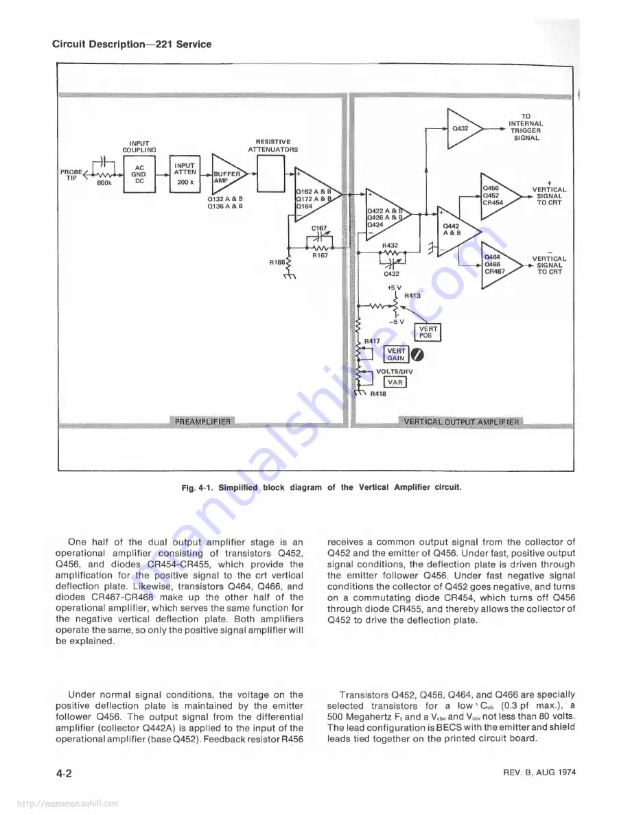
Fig. 4-1. Simplified block diagram of the Vertical Amplifier circuit.
One half of the dual output amplifier stage is an
operational amplifier consisting of transistors Q452,
Q456, and diodes CR454-CR455, which provide the
amplification for the positive signal to the crt vertical
deflection plate. Likewise, transistors Q464, Q466, and
diodes CR467-CR468 make up the other half of the
operational amplifier, which serves the same function for
the negative vertical deflection plate. Both amplifiers
operate the same, so only the positive signal amplifier will
be explained.
Under normal signal conditions, the voltage on the
positive deflection plate is maintained by the emitter
follower Q456. The output signal from the differential
amplifier (collector Q442A) is applied to the input of the
operational amplifier (base Q452). Feedback resistor R456
receives a common output signal from the collector of
Q452 and the emitter of Q456. Under fast, positive output
signal conditions, the deflection plate is driven through
the emitter follower Q456. Under fast negative signal
conditions the collector of Q452 goes negative, and turns
on a commutating diode CR454, which turns off Q456
through diode CR455, and thereby allows the collector of
Q452 to drive the deflection plate.
Transistors Q452, Q456, Q464, and Q466 are specially
selected transistors for a lo w ' Cob (0.3 pf max.), a
500 Megahertz Ft and a Vet™ and Vcev not less than 80 volts.
The lead configuration is B ECS with the emitter and shield
leads tied together on the printed circuit board.
4-2
REV B, AUG 1974
h ttp ://m Q n o m a n .s q h ill.c o m


