Page 4 of 6 Rev 1
February 3, 2020
DRB-480 Handbook
DDA Series Instruction Manual
If the Remote Sense feature is not being used, the Sense terminals should be connected directly to their respective
Vo(+) terminals to avoid additional voltage droop.
4.6 Power Good Signal (PGood)
The DDA power supply comes with Power Good signals on each output. When the outputs are within regulation,
Pins 5 and 6 on the Top Side header connector are pulled up internally to a 5.0V by a 10Kohm resistor. When power
is applied to the module but the output voltage is typically more than
±
12% of the nominal voltage set point due to
input under voltage, over temperature, over load, or loss of control, the Power Good signals will be pulled to ground
through a 75-ohm maximum impedance. If the Power Good feature is not used, the pins should be left open. A
voltage source should not be applied to these pins. LEDs (e.g. “VO1 OK”, “VO2 OK”) on the front panel provide a
visual status indicator of the Power Good signals.
4.7 Over Current Protection ( OCP )
Hiccup mode with automatic recovery.
OCP function operates when the output current exceeds OCP specification. The output will be automatically
recovered when the overload condition is cancelled. Short circuit puts the power into hiccup mode.
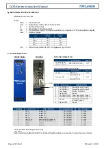
4-8. Output Ripple & Noise
The standard specification for maximum ripple value is measured according to the measurement circuit below. When
load lines are longer, ripple becomes larger. In this case, electrolytic capacitor, ceramic capacitor, etc. might be
necessary to use across the output screw terminals. The output ripple cannot be measured accurately if the probe
ground lead of the oscilloscope is too long. The scope probe and ground lead should be placed
150mm from the
output screw terminal. Use scope probe jacks as much as possible.
Oscilloscope
Bandwidth : 20MHz
+
-
P.S.
C1 C2
Load
1.5m 50
Cable
150mm
C1 : 100uF Electrolytic Capacitor
C2 : 0.1uF Film Capacitor
+
4-9. Series or Parallel Operation
Series or parallel operation is not supported.
4-10. Isolation Test and Withstand Voltage
The DDA series is a non–isolated product.
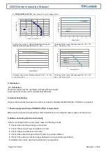
4.11. Output Derating
For
DDA250N-S1PX-12-001
(Single Output) and
DDA500N-D2PP-1205-001
(Dual Output)
0
5
10
15
20
25
25
35
45
55
65
75
85
95
105
O
u
tp
u
t C
u
rr
e
n
t (
A
)
Ambient Temperature (°C)
5Vout
12Vout
15Vout
0
5
10
15
20
25
0
5
10
15
20
25
O
u
tp
u
t C
u
rr
e
n
t 1
(
A
)
Output Current 2 (A)
Ta=30 °C
Ta=40 °C
Ta=50 °C
Ta=60 °C
Ta=70 °C
Typical output current vs. ambient temperature derating per
indicated output voltage setpoints at Vin = 24V.
Combined Output current derating example for Vo1 = 12V;
Vo2 = 5V at Vin = 24V.
C1 : 100 µF Electrolytic Capacitor
C2 : 0.1 µF Ceramic Capacitor

