TCL L65P8M Series Service Manual Download Page 43

GND

T

GND

GND

GND

GND

GND

GND

EN

BOOT

FB

VIN

GND

LX

T

GND

T

GND

GND

GND

GND

NC

LX

EN

SGND

PGND

VIN

PG

FB

GND

GND

T

GND

.............

DESIGNATION

NAME

Last modif

DESCRIPTION

DATE

DRAWN

CHECKED

ON:

BY:

BY:

ON:

PAGE:

OF  :

1

2

3

4

5

6

7

8

9

10

11

12

H

G

F

E

D

C

B

A

12

11

10

9

8

7

6

5

4

3

2

1

THIS DRAWING CANNOT BE COMMUNICATED TO UNAUTHORIZED PERSONS COPIED UNLES S PERMITTED IN WRITING

FORMAT DIN A1

H

G

F

E

D

C

A

Index-Lab

Last saved :

TCL Thomson Electronics Singapore Pte. Ltd.

8 Jurong Hall Road #28-01/06

The JTC Summit SINGAPORE 609434

Tel (65) 63092900 Fax (65) 63092999

TCLNO:

SBU :

DESIGNATION

GND

GND

GND

GND

GND

GND

GND

GND

GND

GND

GND

GND

GND

GND

GND

GND

GND

T

T

T

T

GND

T

T

T

T

LX2

GND3

VCC

NC2

BYP

FB

ILMT

TEST

EN

NC1

PG

GND2

GND1

LX1

IN4

IN2

IN1

BS

LX3

IN3

GND

T

T

T

GND/ADJ

OUT

VIN

4

GND

GND

T

FB

IN

LX

GND

EN

GND

GND

GND

EN

VBST

VFB

VIN

GND

SW

EN

VOUT

PVCC

SW

SCL

VIN

SDA

BOOT

T

T

GND/ADJ

OUT

VIN

4

T

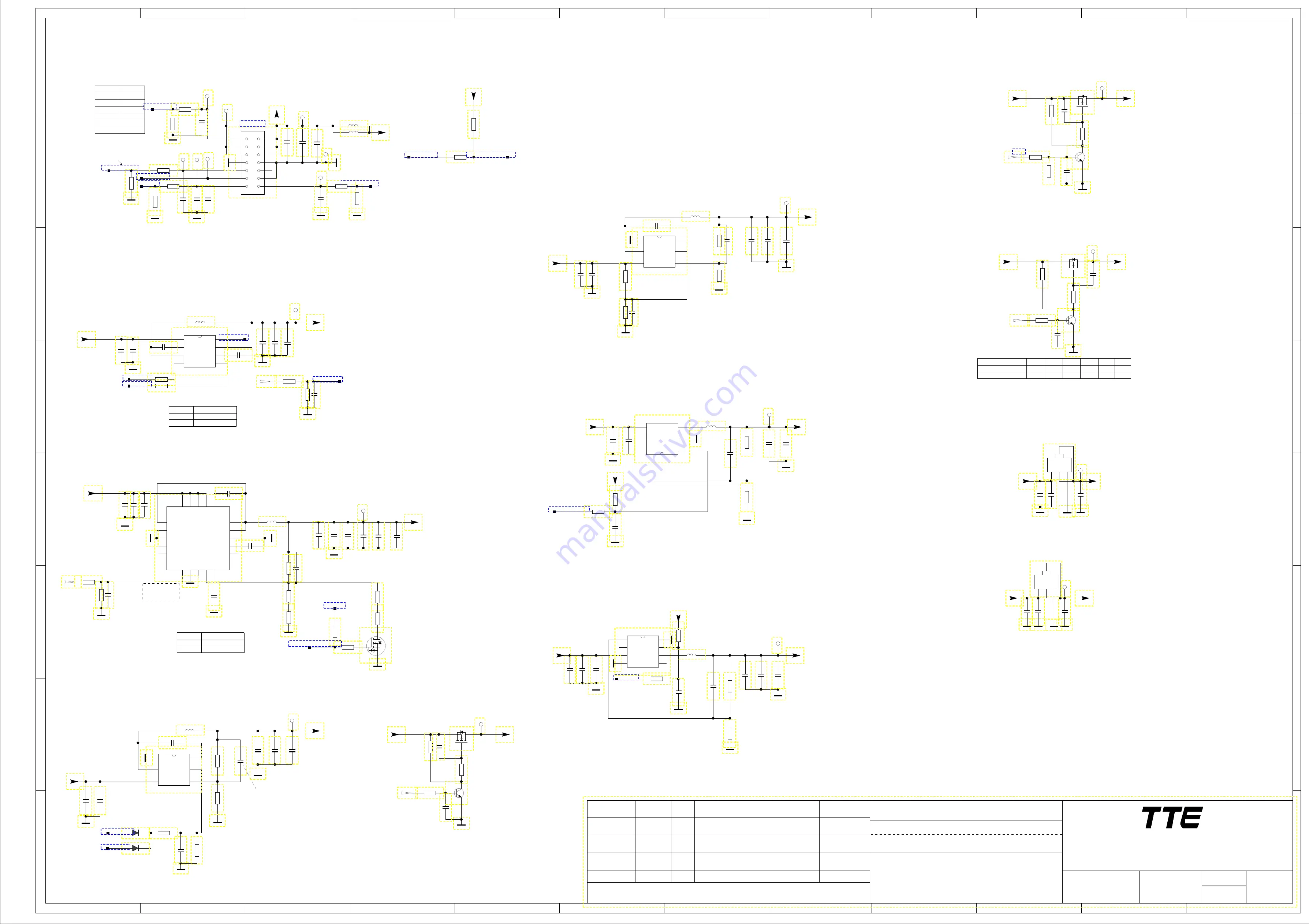
WHEN FAR-FIELD SPEECH ON,DMIC_ON=HIGH
WHEN FAR-FIELD SPEECH OFF,DMIC_ON=LOW

KEY = 2.85(TYP) (>2.2V) DMIC ON

KEY = 1.01(TYP) (0.8-1.2V) DMIC OFF

@1A   max

@1A   max

r=62%

Vref=0.765V

@max 2A

(4.5V-18V)

VEN=1.43V(on),1.21V(off)

12V TO 5V

MOUNT CDA4=10PF,for DCDC noise

Fsw=500k

(Vin=2.7-6V)

max3A

Vref=0.6V

EN=1.5V(on),0.4V(off)

(RDson=100/70)

(FREQ=1MHz)

3V3_STB TO DDR_1V5

0603

Vref=0.768V

EN=1.6V(on),    0.8V(off)

Fsw=580KHz

(Vin=4.5V-17V)

@max 3A

r=42%

12V TO 3V3_STB

Pseudo Fsw=600KHZ

ILMT=float, 10.3A

ILMT=0, 7.8A

ILMT=1, 13.3A

Vref=0.6V

EN=1V(on),0.4V(off)

0.488A

0.98A

1.488A

1.98A

2.47A

2.98A

vin=3.3V,    drop Voltage

0.032V

0.069V

0.029V

0.058V

0.091V

0.124V

0.162V

0.213V

0.108V

0.150V

0.200V

0.270V

vin=5V,        drop Voltage

@1A   max

max1A

(Vin=2.5V-6.5V)

r=32%

12V

12V

12V

12V

12V

GND

GND

3.3VSB

A_DIM

BL_ON

GND

P_DIM

Must controlled by PWM

POWER_ON

5V TO TUNER_3V3

(6)

3V3_STB TO ST_A1V0

(Vin=4V~23V)

1.5V(on)

0.4V(off)

(6)

(6)

Fsw=1.5MHz

Vref=0.6V

3V3_STB TO 3V3VD

(Vin=4.5V-18V)

EN=2V(on), 0.4V(off)

@max6A

12V TO CORE_1V0

12V TO CPU_1V0

3V3VD TO 1V8

BL_BST

Power Connector(12V)

Only for 12V(14PIN)

when 24V in,NC PJ1

when 24V in,NC this module

VID_H

VID_L

Vout

1.05V(+/-0.03V)

CORE POWER

CPU(DVFS)

VID_H

VID_L

Vout

1.15V(+/-0.03V)

0.98V(+/-0.03V)

0.95V(+/-0.03V)

@max 6A

3V3_STB TO DMIC_3V3

RV20

22K

/NC

18K

RV21

/NC

B

C

E

LMBT3904LT1G

QV6/NC

RV19

22K

/NC

22K

RV18

/NC

CV14

1U

/NC

G

D

S

QV5

PMV65XP

/NC

CV15

0.1U

NC/

CW12

1U

5V_FAR

RDA7

47K

RDA4

10K

1

2

3

4

UDD

AS1117-3.3

CDC13

220P

NC/

CDL4E

22P

RDC8

120K

RDBC1

47K

33K

RDF4

RDC9

22K

B

C

E

LMBT3904LT1G

QW2

LW2 220R

LW1 220R

CW9

0.1U

NC/

CW11

10U

CW10

10U

CPU_1V0

CPU_1V0

CORE_1V0

RW16

22K

1

2

3

6

5

8

4

7

UDH

RT6203E

5

6

4

3

1

2

UDBC

TPS563201

G

D

S

QW1
PMV65XP

LDL1E
1.5UH

CDL8E

0.01U

CDL7E

0.1U

CDL6E

22U

CDL5E

22U

CDL3E

0.1U

CDL2E

10U

3V3_STB

CDL1E

10U

CW7

0.1U

RDH1

100R

RDH2

100R

1

2

4

6

8

12

14

10

3

5

7

9

11

13

PJ1

22K

RDF2

22K

RDL5E

RDL3E

33K

RDBC4

15K

51K

RDBC3

RDC7

1K

4K7

RDC6

RDC5

820R

RDC4

12K

RDC3

7K5

CDC12

0.1U

CDH7

0.1U

CDI2

0.1U

CDF5

0.1U

QDC1

NX7002AK

CW5

0.01U

12V_IN

5

4

3

2

1

UDF

AN_SY8077

CDF1

10U

BL_ON_1

A_DIM

RW14

220R

12V_IN_1

3V3_STB

SCPU_EN

0.047U

CDH2

CDH1

10U

0.1U

CDH3

CDH4

1U

22U

CDH6

22U

CDH5

LDH1

1.5UH

12V

I2C-SCL

I2C-SDA

CDI3

10U

10U

CDI1

NC/

CDC3

0.047U

10U

CDC2

CDC1

10U

10U

CDD1

CW6

0.01U

CDC14

10U

CORE_1V0

SCPU_EN

POWER_ON

3V3VD

1

2

3

4

UDI

AS1117-1.8

TUNER_3V3

3V3VD

ST_A1V0

3V3_STB

5V

CDF6

0.01U

RDF5

10K

CDBA4

0.01U

3V3_STB

RDF1

220R

RW17

22K

22K

RW15

CDF4

22U

CDF3

22P

LDF1

2.2UH

CDF2

0.047U

CDC5

1U

0.01U

CDC4

RDC2

10K

NC/

RDC1

220R

22U

CDC11

CDC10

22U

CDC9

22U

CDC8

22U

2U2

CDC7

LDC1

0.68UH

CDC6

0.1U

19

18

17

16

15

14

13

12

11

10

9

8

7

6

5

3

2

1

20

4

UDC

SYT286A

10K

RDBA2

NC/

RDBA1

220R

CDD3

10U

0.1U

CDD2

NC/

2K2

RW13

10K

RW8

220R

RW7

CW4

0.01U

CW3

0.01U

CW2

1000P

10K

RW6

220R

RW5

10K

RW4

220R

RW3

CW1

1000P

10K

RW2

RW1

220R

12V_IN

GND

GND

3V3_STB

POWER_ON

12V

1V8

3V3VD

POWER_ON

12V

A_DIMMING

ST_A1V0

BL_ON

POWER_ON

1V8

GND

POWER_ON

GND

GND

ADIM

PDIM

GND

GND

GND

BL_BST

TUNER_3V3

P_DIM_PSU

BL_BST

BL_BOOST

BL_ON

P_DIMMING

POWER_ON_OUT

GND

GND

POWER_ON

WOL_PWR_EN

CDBC1

10U

22P

CDBC5

NC/

3V3_STB

22U

CDBC7

CDBC6

22U

3.3UH

LDBC1

0.1U

CDBC4

CDBC3

0.01U

10K

RDBC2

0.047U

CDBC2

3V3_STB

12V

GND

GND

GND

3V3_STB

10K

RDL1E

RDL2E

220R

5

6

7

8

4

3

2

1

UDLE

RT5797A

DDR_1V5

DDR_1V5

STR_EN

CORE_SCPU_VID

3V3VD

CDBC8

0.1U

12V_IN

DW2

1N4148WS

DW1

1N4148WS

POWER_ON

RDA1

220R

CW13

0.1U

NC/

B

C

E

LMBT3904LT1G

QW4

G

D

S

QW3
PMV65XP

RW10

22K

RW11

22K

22K

RW9

5V

CDA4

10P

CDA5

10U

CDA2

0.047U

CDA1

10U

RDA3

56K

CDA7

0.1U

CDA8

0.01U

CDA6

10U

LDA1

4.7UH

CDA3

0.1U

5

6

4

3

1

2

UDA

RT6212A

12V

5V_FAR

5V

5V_FAR

POWER_ON

DMIC_ON

KEY

DMIC_3V3

DMIC_3V3

3V3_STB

KEY

Summary of Contents for L65P8M Series

Page 1: ...3 Alignment Procedure 4 Block diagram 5 Scheme Diagram 6 Troubleshooting SORGH GUDZLQJ This m anual i s t he l atest at t he t ime of pr inting and doe s not include the modification which may be mad...

Page 2: ...ectric shock to the person The exclamation point within an equilateral triangle is intended to alert the user to the presence of important operating and maintenance servicing instructions in the liter...

Page 3: ...impact of any kind Be particularly careful not to damage the picture tube surface 9 Unplug this television set from the wall outlet before cleaning Do not use liquid cleaners or aerosol cleaners Use...

Page 4: ...ng conductors location of antenna discharge unit connection to grounding electrode and requirements for the grounding electrode 15 2 Note to CATV system installer Only for the television set with CATV...

Page 5: ...durein youroperatinginstructions do not attempt any further adjustment Unplug the set and call your dealer or service technician 22 Whenever the television set is damaged or fails or a distinct change...

Page 6: ...ng Angle H V 178 178 Ethernet Network Life Time Typ 30 000hrs LED Indicator Status Below the middle of the frame White in Standby Color 1 07B 10bit Normal Flashing Off Refresh Rate 60Hz Button on Pane...

Page 7: ...Google Play Movies and TV and Music etc Google Play store Many apps in the Google play store Streaming channels Google Play Movies and TV Chromecast A better way to get your video music and games to y...

Page 8: ...ment Specification for RT2851 Series v0 01 docx Page 1 of 31 TCL World Wide R D FPD CENTER Test Alignment Specification TAS for RT2851 Series Version0 01 PREPARED BY DATE 2018 12 14 CHECKED BY DATE AP...

Page 9: ...mation contained in this document is proprietary to TCL SZ FPD lab and shall not be disclosed by the recipient to third persons without the written permission of the team leader or GM of R D Revision...

Page 10: ...480i p 576i p 720p up to 2160p compliant v2 0 with HDCP2 2 2R 2xHDMI2 0a 4K 60Hz YUV4 2 0 2S 2xHDMI2 0a 4K 60Hz YUV4 4 4 1S MHL 1S ARC VGA VGA DVI audio CMP YPbPr can support from 480i up to 1080p aud...

Page 11: ...A IC Details Position IC Details Position Market RT51HS EU Main SW EMMC 8GB 16GB BIN image UE1 16GB V8 R851T02 LF1V001 HDMI SWITCH EDID BIN image HDMI EDID and HDCP Embedded in main chip Include in ma...

Page 12: ...Test and Alignment Specification for RT2851 Series v0 01 docx Page 5 of 31 HDMI to USB and HDMI to HDMI cables The wire connecting the TV to the adapter is shown below HDMI USB HDMI HDMI...

Page 13: ...check the voltage according to the relevant block diagram circuit diagram and voltage specification For example check SoC voltage AVDD3V3 DVDD3V3 VCCK_1V0 AVDD1V0_STB 095VM 3V3SB etc DDR voltage DDRV_...

Page 14: ...n following presets 115200 8 n 1 Once initialized PS caption is toggle displayed on bottom left screen S like Serial To communicate with TV depending on SIACP revision layout implementation you need t...

Page 15: ...4 22KHz Tone Range Frequency 20 5KHz 23 5KHz Amplitude 400mV 900mV Current 400mA SPDIF Audio Amplifier PCM or Dolby D PCMCIA CI CAM card adaptor Conax Irdeto Viaccess CMP via mini jack adaptor YPbPr A...

Page 16: ...ix How to upgrade CI Key using USB See Appendix How to upgrade Widewine Key using USB See Appendix How to upgrade PlayReady Key using USB not support at this time See Appendix How to upgrade HDCP key...

Page 17: ...LAN test can be done by connecting DHCP server to TV s RJ45 and check that IP subnet mask DNS addresses are visible on Settings Network IP settings Ethernet More in depth test can be performed faster...

Page 18: ...ey run the function Press RCU Exit key exit the Factory menu Factory Captions Description While Factory hotkey is enabled there re some toggled display information 2s relative to SW ProjectID CI Netwo...

Page 19: ...gnment Golden sample As some color coordinates discrepancies can be noticed from panel batches to others it may necessary to perform slight touch up For Color temperature adjustment switch TV on leadi...

Page 20: ...the probe on the middle of the panel then run main vi The 4 3 gamma will be created and calibrated automatically and saved in the TV As 4 3 gamma is a new and good way for PQ especially for HDR we nee...

Page 21: ...at can be copied on demand to all further TV production lot of same TV To access cloning function you can select Factory menu USB Clone Scroll down to TV to USB or USB to TV and press RCU OK key to pr...

Page 22: ...able Factory HotKey After that selecting Factory menu Reset Shop then pressing RCU OK key Other faster methods via UART IR commands are available on enclosed SIACP requirements rev v8 31 Note A passwo...

Page 23: ...ification for RT2851 Series v0 01 docx Page 16 of 31 3 Close the serial port tool open the rtice software select the Burn page as shown below 4 Click the settings icon open the settings page and confi...

Page 24: ...ion for RT2851 Series v0 01 docx Page 17 of 31 Connect Type select RS232 Comm port selects the corresponding serial port Set Status type option ROM Code IC Type Selection RTD2851 Then click ok 5 Seria...

Page 25: ...t and Alignment Specification for RT2851 Series v0 01 docx Page 18 of 31 Select connect Sucess 6 Select the Burn burn_Direct Configure Burn parameters and select bootcode bootcode_for_rtice bin load p...

Page 26: ...fication for RT2851 Series v0 01 docx Page 19 of 31 as shown below 7 Click the Start button to enter the boot state and the state will change to the connect state as shown below 8 After the burn is su...

Page 27: ...rboot rescue exe bin change to input fatload usb 0 4 0x1500000 dvrboot rescue exe bin go 0x1500000 Then Upgrade Main SW Copy Main SW Update img into USB stick pen drive root path Insert USB to TV USB...

Page 28: ...o change Project ID with RCU Process following subsequence IR codes to change projectID 062598 xxx xxx ProjectID ex 001 If it works the TV will restart automatically Appendix How to upgrade CI Key usi...

Page 29: ...it means burn the key success After burning the HDCP key will movie to the folder HDCP_BACKUP HDCP2 0 Create the folder named HDCP2 change the HDCP2 0 key to HDCP2_xxx bin xxx is the number put HDCP2...

Page 30: ...ess router or modem and a Wireless LAN Adapter Select Menu Network Settings Wi Fi On then it will appear the valid wireless networks near your area Select available access pointand press OK to connect...

Page 31: ...mode by pressing key then press EXIT key to activate it Press Menu key on local keyboard to exit the Burning mode Note Factory Hotkey submenu must be ON 3 Reset Shop submenu Item Sub item Value Note R...

Page 32: ...ding on Cloning mode 7 Preset Factory Channel submenu Item Sub item Value Note Preset Factory Channel Factory Area HZ PL Choose the factory area Channel Preset Preset TV Channel 8 DeviceID Test submen...

Page 33: ...Close ADB Service menu submenu Item Sub item Value Note 0 Project SN Project SN 1 EPolisy Number EPolisy Number 2 Hardwarel Hardwarel 3 Software Software Version 4 ProjectNa me Project Name 5 frcVers...

Page 34: ...Param setting submenu Item Sub item Value Note 0 Sound Setting Sound mode Music Movies News Standar d User Switch soundmodeby pressing key Balance 0 100 Adjust sound balanceby pressing key Auto audio...

Page 35: ...de 0 2 Switch nature light modeby pressing key APL1 0 255 Adjust value ofAPL1by pressing key APL1_BL 0 255 Adjust value of APL1_BLby pressing key APL2 0 255 Adjust value of APL2by pressing key BP 0 25...

Page 36: ...ng key Option menu depend on model ini with opposite Project ID Format in model ini Factory PictureModePreset STANDARD VIVID MILD STUDIO USER DYNAMIC STADIUM CINE MA SOUND MODE Music Movie News Standa...

Page 37: ...etup of white balance Firstly you need to enable Factory Key Press RCU MENU key to display main menu Select Settings Picture Advanced setting Contrast Scroll down to Contrast item Press the subsequenc...

Page 38: ...Test and Alignment Specification for RT2851 Series v0 01 docx Page 31 of 31 After burning the MGK key will movie to the folder MGKKEY_BACKUP Note The operation must enable factory P mode...

Page 39: ...nRT51 Block diagram...

Page 40: ...nRT51 Chassis Block Diagram...

Page 41: ...nPower supply Block Diagram...

Page 42: ...The JTC Summit SINGAPORE 609434 Tel 65 63092900 Fax 65 63092999 TCL Thomson Electronics Singapore Pte Ltd 8 Jurong Town Hall Road 28 01 06 TCLNO DESIGNATION Component UDH 6203E MX661 I2C Address 0x68...

Page 43: ...C B C E LMBT3904LT1G QV6 NC RV19 22K NC 22K RV18 NC CV14 1U NC G D S QV5 PMV65XP NC CV15 0 1U NC CW12 1U 5V_FAR RDA7 47K RDA4 10K 1 2 3 4 UDD AS1117 3 3 CDC13 220P NC CDL4E 22P RDC8 120K RDBC1 47K 33K...

Page 44: ...0 01U 19 11 16 17 8 7 6 5 4 3 2 1 13 24 14 23 22 21 20 18 15 9 10 12 UT1 MXL661 CS42 0 047U CS46 10U 5 6 7 8 4 3 2 1 US30 CS40 10U CS47 10U NC DS42 MBRX14 DIF DIF D IF D IF DEM_DIF DEM_DIF RS58 10K RS...

Page 45: ...HDMI3 RX0 HDMI3 RX1 HDMI3 RX2 HDMI3 RXC HDMI2 RXC HDMI2 RXC HDMI2 RX0 HDMI2 RX0 HDMI2 RX1 HDMI2 RX1 HDMI2 RX2 HDMI2 RX2 HDMI1 RXC HDMI1 RX0 HDMI1 RX0 HDMI1 RXC HDMI1 RX1 HDMI1 RX2 HDMI1 RX1 HDMI1 RX2...

Page 46: ...3P3 CN1 0 1U CN2 0 1U 1 3 5 6 4 2 PN1 RN48 0R RN60 33R B E C LMBT3906LT1G QN1 5 4 1 3 2 PN40 22K RN41 22K RN40 RN77 22K NC CN42 0 047U CN45 0 047U 1 2 DN41 1 2 DN40 10K RN43 75R RN46 100R RN47 3P3 CN7...

Page 47: ...TCON7 GPIO95 TCON8 GPIO96 TCON9 GPIO97 TCON10 GPIO98 TCON11 GPIO99 NF_CE0 ST_GPIO46 NF_ALE ST_GPIO44 POL_EN_N NF_CLE ST_GPIO45 SPI_DO GPIO88 SPI_CSN GPIO85 SPI_DI GPIO84 SPI_WP GPIO83 SPI_SCLK GPIO87...

Page 48: ...4 6 7 8 9 10 11 13 14 15 12 22 21 20 19 18 17 16 34 33 32 31 30 29 28 27 26 25 24 23 67 66 65 64 63 62 61 60 59 58 57 56 55 54 53 52 51 50 49 48 47 46 45 44 43 41 40 39 38 37 36 35 68 42 PJ60 1V8 EMMC...

Page 49: ...O SPEAKER PORT 8ohm Speaker CA23 CA30 use 0 22u 28 BB0224 KBX 6ohm bass CA23 CA30 use 0 47u 28 BB0474 KBX C0805 2 1 PA2 2 1 PA1 CA33 1U NC CA2 10U CA3 1U CA32 1000P 1000P CA31 1000P CA25 CA24 1000P 12...

Page 50: ...0 1U CJ48 0 1U CJ46 0 1U 0 01U CJ14 CJ13 0 01U LD_MTX_SRX I2C SDA P I2C SCL P 3V3VD RJ33 10K NC RJ32 10K NC RJ31 10K NC RJ30 10K NC LD_MRX_STX LD MTX SRX LD MRX STX LD_SPI_CK PANEL_VCC I2C WP I2C SCL...

Page 51: ...nRT51 Key Components 5V 1V5 PANEL_VCC 12V 12V 3V3 PW_ON P_DIM A_DIM 3V3STB 1V8 TUNER_3V3...

Page 52: ...nRT51 Key Components UDE1 3 3V TO 1V UDBC 12V TO 3 3V UDLE 3 3V TO 1 5V UDC 12V TO CORE 1V UDD 5V TO 3 3V UDI 3 3V TO 1 8V AMP82088 UE1 EMMC UDA 12V TO 5V UDC 12V TO CPU 1V...

Page 53: ...nKey Test Point Main Power Supply Normal Abnormal 12V 1 Check the impedance if short to GND 2 Check if the power supply board is work 12V 12V Test point...

Page 54: ...nKey Test Point DC to DC UDBC 12V to 3V3_STB UDF 3V3_STB to ST A1V0 12V LDBC1 3V3_STB LDF1 ST A1V0...

Page 55: ...nKey Test Point DC to DC UDBC 12V to 3V3_STB 12V LDBC1 3V3_STB UDBC PIN Impedance Voltage 1 0 0V 2 17K 3 3V 3 1M 12V 4 12K 0 7V 5 9K 2V 6 OPEN 8 7V...

Page 56: ...nKey Test Point DC to DC UDF 3V3_STB to ST A1V0 LDF1 ST A1V0 UDF PIN Impedance Voltage 1 0 3 3V 2 17K 0V 3 1M 0 99V 4 12K 3 3V 5 9K 0 59V...

Page 57: ...nKey Test Point STR Enable UDLE 3V3_STB to 1V5_DDR 3V3_STB LDL1E 1V5_DDR UDLE PIN Impedance Voltage 1 13 2K 0 5V 2 NC NC 3 16 1K 3 3V 4 0 0V 5 NC NC 6 1 3K 1 48V 7 24K 3 3V 8 0 0V...

Page 58: ...CORE 1V0 UDC PIN Impedance Voltage PIN Impedanc e Voltage 1OPEN 4 23V 1121K 3 27V 238K 12V 12 00V 338K 12V 13NC 0V 438K 12V 144 5K 0 58V 538K 12V 15OPEN 0V 6 00 9V 16NC 7 00V 17OPEN 3 27V 8 00V 18OV 0...

Page 59: ...nKey Test Point UDA 12V TO 5V LDA1 5V_FAR QW3 5V UDA PIN Impedance Voltage 1 0 0V 2 57 6K 5 1V 3 10K 12V 4 9 5K 0 7V 5 38 5K 2 82V 6 OPEN 9 6V...

Page 60: ...erent LNB voltage output 13 5V min13 3V max14 2V For vertical polarization V 18 5V min17 7V max19 2V For horizontal polarization H nKey Test Point minimum US2 12V to 13 5V or 18 5V LNB VCC US30 JS32 L...

Page 61: ...est Point Reference voltage GND Input voltage 5V UDD ouput TUNER_VCC 3V3 UDD TUNER VCC 3V3 5V UDD PIN Impedance Voltage 1 0 0V 2 1K 3 3V 3 52K 5V 4 1K 3 33V When UDD is failure The bad symptoms of TV...

Page 62: ...LDO 19 nKey Test Point Reference voltage GND Input voltage 3V3_NORMAL U202 ouput 1V8 UDI 1V8 3V3VD UDI PIN Impedance Voltage 1 0 0V 2 1K 1 77V 3 52K 3 33V 4 1K 1 77V...

Page 63: ...POWER SWITCH nKey Test Point 3V3_NORMAL SWITCH QW2 G POWER_ON QW1 D 3V3_NORMAL QW2 S 3V3_STB QW2 B normal voltage 0 59v Power_on 3 25v QW2 C normal voltage 0 04v...

Page 64: ...nKey Test Point PANEL_VCC 12V QJ31 PANEL_VCC...

Page 65: ...nKey Voltage Test Point Key Voltage for RTD2851 RTD2851 POWER normal 3 3V POWER pressed 0V...

Page 66: ...5 Jun 19 Page 30 nImpedance Test UA1 Amplifier RA6 RA7 RA8 RA9 RA10 RA15 SOC 3 3M 3 3M 3 3M 67K 67K 162K AMP 3 3M 3 3M 3 3M 67K 67K 162K...

Page 67: ...nTrouble Shooting...

Page 68: ...nTrouble Shooting...

Page 69: ...nTrouble Shooting...

Page 70: ......

Reviews: