background image

T

GND

T

T

GND

GND

GND

BOOT

EN/SYNC

PVCC

FB

GND

SW

VIN

TTH

T

GND

GND

GND

GND

GND

GND

GND

GND

GND

GND

T

T

T

T

GND

GND

GND

GND

D1B

D1A

G2

G1

S2

D2B

D2A

S1

T

A

3

2

1

F

E

D

C

B

8

7

6

5

5

4

3

2

1

THIS DRAWING CANNOT BE COMMUNICATED TO UNAUTHORIZED PERSONS COPIED UNLES S PERMITTED IN WRITING

F

E

D

C

B

A

4

6

7

8

FORMAT DIN A2

NOTE:

PAGE:

OF

TCL

GND/ADJ

OUT

VIN

4

GND/ADJ

OUT

VIN

4

T

T

T

T

GND

T

GND

GND

GND

T

T

GND

GND

T

T

GND

T

IN

ILIM

LG

BST

SW

HG

GND

REF

SS

FB

T

T

GND

T

PH

GND

EN

VIN

VSENSE

SW4

AGND

VOUT

VCC

NC2

PG

NC1

BST

FB

MODE

EN

SW2

PGND

SW3

VIN

SW1

T

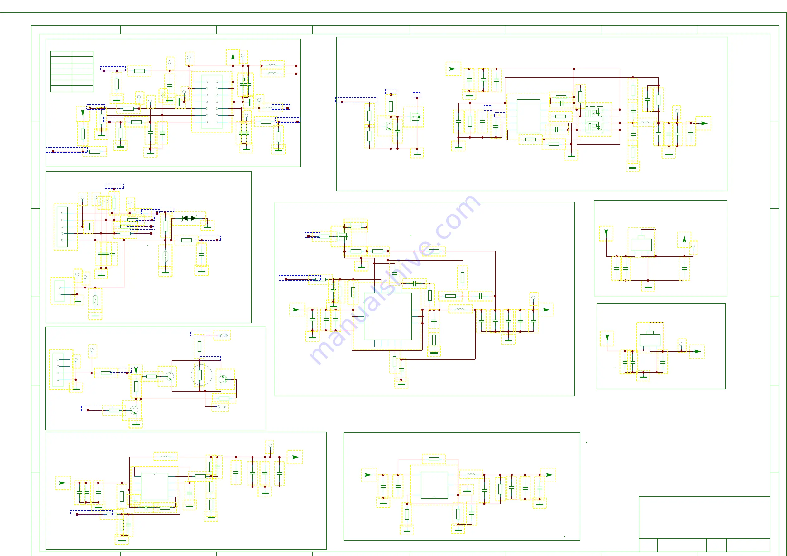
3D Switch Control Circuit

Fsw=500KHz

Vref=0.8V

(Vin=4.5V-17V)

max3A

Vref=0.6V

Fixed Fsw=500KHZ

(Vin=5V-24V)

@max5A

Fixed OCP=7.5A

Vref=0.8V

@max0.5A

(Vin=4.5V-17V)

Fsw=600KHz

Must controlled by PWM

12V

3.3VSB

GND

GND

DIM_DC

DIM_PWM

Vref=0.59V

Change RD85 and CD83 to adjust Fsw, Set Fsw=500kHZ

(Vin=3V-28V)

LDO

@max5A

Change RD80 to adjust OCP,Set OCP=7.6A

12V

12V

If Input Voltage=24V,CD80/CD81=2.2uF/50V,RD85=47K,CD8A=1000P,RD88=6R8

If Input Voltage=12V,CD80/CD81=10uF/16V,  RD85=36K,CD8A=3900P,RD88=2R2

@max 320mA

5V to 3.3V LDO circuit

5V to 2.5V LDO circuit

Without via on net KEY_IN

The distance between different net via>2mm

POWER_ON

BL_ON

GND

12V

3D_CTRL

12V

Changed by Frank/20140929

Core Power

12V to 3.3V DC-DC circuit

12V to 1.15V DC-DC circuit

12V to 5V DC-DC circuit(standard MP2905 circuit)

12V to 1.5V DC-DC circuit

5pin IR&Key Port

14Pin DC Power Port

12V

GND

L003

220R

2

1

P002

1

2

3

4

5

P003

1

2

4

6

8

12

14

10

3

5

7

9

11

13

P001

3D_PWM

CDB4

1U

16

14

7

11

5

4

3

10

12

6

13

9

2

15

1

8

U008

MP8765

RDB3

470R

LDB0

1UH

3

2

1

4

5

UDG1 TPS560200

3V3SB

3D_CTRL

B

C

E

Q803

BT3904

3D_DIM

470R

R829

3D_DIM

R817

10R

3D_DIM

B

C

E

Q802
BT3904

3D_DIM

B

C

E

Q801
BT3904

3D_DIM

R815

4K7

3D_DIM

470R

R828

3D_DIM

4K7

R816

3D_DIM

1

2

3

4

P103

NC

3D_DIMMING

10K

R052

1V5_DDR2

GND

RDG2

15K

3V3SB

RDG1

100K

3V3SB

CDG6

33P

NC

RDG4

47K

3V3SB

0.01U

CDG7

3V3SB

RDG5

47K

3V3SB

100K

RDB0

NC

RDB9

47K

R009

3K3

CDBC

220P

NC

RDB5

4R7

RDBA

0R

NC

470R

R060

R007

1K

NC

LOGO_OUT

1K

R020

LED_OUT

120R

L017

3V3SB_1

3V3SB

3V3SB

R067

33K

R068

33K

RDB6

10K

RDB2

56K

RDB1

51K

9

10

5

6

7

8

4

3

2

1

MP2905

UD80

0.1U

C006

GND3

KEY1

KEY

F002

F001

GND

CDB2

0.1U

220R

R079

CDG5

0.1U

3V3SB

10U

CDG4

3V3SB

CDG3

10U

3V3SB

LDG1

10UH

3V3SB

CDG2

0.1U

3V3SB

CDG1

10U

3V3SB

R069

4K7

Q001

2N7002K

VDDC1V15

B

C

E

Q003

BT3904

C009

1000P

POWER_ON_OUT

POWER_ON_OUT

SS

6800P

CD83

REF

10U

CD8B

10U

CD8D

L011

220R

A_DIM

GND

10K

R073

6.8UH

LD80

0.1U

C090

GND

16V

470U

C093

USE CONDITION DC=12V

5V

12V

12V_1

1000P

C092

0.01U

C099

0.01U

CD84

L010

220R

0.1U

C012

C061

0.1U

10U

C025

3V3

C008

10U

C019

10U

C021

0.1U

3V3SB

C007

0.1U

1

2

NC

PESD5V0S1BL

D001

R014

22K

2V5

2V5

2K2

R074

0.1U

CD8E

10K

RD8A

RD8B

10K

10U

CD80

POWER_ON

GND

3D_EN_1

BL_ON

GND

10K

R078

3V3SB

0.1U

CD82

10U

CD8C

2R2

RD86

CD8A

3900P

36K

RD85

6R8

RD82

6R8

RD81

10U

CD81

R071

10K

R070
220R

GND

3V3

4K7

RD80

12V_M

5V

1

2

3

4

U003

AS1117-3.3

1

2

3

4

U002

AS1117-2.5

GND

...........

TEL:+86 755 33312403

NANSHAN DISTRICT.SHENZHEN.GUANGDONG 518067 CHINA

5TH FLOOR.TCL BUILDING.SOUTH NANHAI ROAD

WW R&D CENTER TCL MULTIMEDIA TECHNOLOGY HOLDING LTD.

5V

5V

8

7

6

5

2

4

1

3

A04832

QD80

1K2

RD83

0.1U

CD87

0.01U

CD86

150P

CD89

1U

CD88

2U2

CD85

9K1

RD84

GND

10K

R076

0.01U

C087

220R

R072

DIM_DC

DIM

GND

220R

R075

220R

R077

0.01U

C091

GND

0.01U

C088

BL_ON_OUT

0.01U

C011

IR

LED

470P

C014

R015

4K7

KEY_IN

3V3SB

C023

10U

GND

12V_M

3V3SB

Q002

2N7002K

R011

10K

R010

10K

10K

R012

REF

SS

CDBD

220P

CDBB

0.1U

VDDC1V15

CDBA

22U

CDB9

22U

RDB4

1M

CDB5

0.22U

CDB8

22U

CDB7

22U

RDB7

10R

NC

CDB1

10U

CDB0

10U

CDB3

0.1U

12V_M

GND4

IR_IN

VID1

POWER_ON_OUT

RDI4

30K

RDI5

30K

RDI6

4K22

RDI1

47K

22U

CDIA

NC

CDI6

22U

RDI7

3K3

LDI1

2.2UH

NC

22P

CDI5

CDI9

10U

NC

12V_M

RDI2

10R

RDI0

100K

NC

CDI0

10U

0.1U

CDI8

GND

CDI7

22U

5

6

7

8

4

3

2

1

UDI1

RT7296A

0.1U

CDI1

RDI3

82K

0.1U

CDI3

GND

CDI4

0.1U

1V5_DDR

0.1U

CDI2

GND

POWER_ON_OUT

R124

10R

NC

3D_DIMMING

GND_3D_DIM

GND

3D_PWM

5V

DIM_OUT

0R

R825

NC

3D_DIM

3D_DIM_SW

3D_DIM

KEY

BL_ON

POWER_ON

AMP_VCC

DIM_OUT

P_DIM

12V_M

3V3SB

GND_DC

Summary of Contents for L55E5800UDS

Page 1: ...ion 3 Alignment Procedure 4 Block diagram 5 Scheme Diagram 6 Troubleshooting SORGH GUDZLQJ This m anual i s t he l atest at t he t ime of pr inting and doe s not include the modification which may be...

Page 2: ...ectric shock to the person The exclamation point within an equilateral triangle is intended to alert the user to the presence of important operating and maintenance servicing instructions in the liter...

Page 3: ...impact of any kind Be particularly careful not to damage the picture tube surface 9 Unplug this television set from the wall outlet before cleaning Do not use liquid cleaners or aerosol cleaners Use...

Page 4: ...ng conductors location of antenna discharge unit connection to grounding electrode and requirements for the grounding electrode 15 2 Note to CATV system installer Only for the television set with CATV...

Page 5: ...durein youroperatinginstructions do not attempt any further adjustment Unplug the set and call your dealer or service technician 22 Whenever the television set is damaged or fails or a distinct change...

Page 6: ...Angle Typ H V 178 178 EPG Yes Life Time Typ hrs 30 000 Subtitle Closed Caption Yes Color 1 07 billion 10bit Parental Control Yes Refresh Rate 2D 60Hz Sleep Timer Yes System Update Yes Hotel Mode Side...

Page 7: ...Keyboard Wireless Mouse Game Controller 1 pcs PC 8612RF gamestick Batteries L1 mm 1242 4 Diagonal size cm 139 W1 mm 89 7 Slim Edge Design Up mm 14 H1 mm 721 5 Slim Edge Design Bottom mm 14 L2 mm 1029...

Page 8: ...TCL ALIGNMENT ELECTRICAL TEST PROCEDURE MS69KE LA V1 0 CONTENTS Drafted by Checked by Approved By YF Fk07 2013 21...

Page 9: ...E 5 3 3 1 CUT OFF ALIGNMENT 5 3 3 2 White balance 6 4 AUDIO ALIGNMENT 7 5 SHOP INITIAL 7 SHOP INITIAL SHOULD BE DONE AT THE LAST ALIGNMENT 7 6 FACTORY MENU 7 6 1 HOW TO ENTER FACTORY MENU BY REMOTE CO...

Page 10: ...o All the Models is 12V and 3 3V for the Main BD The signal of POWER_ON enables the 12V and the other Voltages as well If POWER_ON signal 0V 12V and the others are not available If POWER_ON signal 3 3...

Page 11: ...To navigate the MENU using KEY Board A To switch on off the TV set Action Press and hold for seconds the main navigation menu pop up Then Press upward or downward to choose and press the button Obser...

Page 12: ...highlighted item Action Press GO BACK key shortcut key Observe User will exit from the selection 2 4 Video functional check 2 4 1 HDMI 2 4 1 1 DVI mode Standard Monitor Format VESA Connect HDMI cable...

Page 13: ...Analog RF signal input Connect Antenna cable to tuner port And the TV standard is NTSC M Change the display source to TV Channels The Tuner has two inputs they are Antenna and Cable 2 4 2 2 Digital R...

Page 14: ...t to make sure the Project ID is correct Alignment Conditions In order to have defined conditions for the alignment procedure the TV set should be warmed up for 10 minutes 3 1 ADC Calibration MS1368K...

Page 15: ...djust G offset 128 0 Not need to adjust B offset 0 255 127 127 Need to adjust The default values have a close relation with panel brightness After white balance alignment a picture performance check s...

Page 16: ...re Menu Then inside Picture Setting Menu And move the cursor to Vedio select Contrast item Press the Password 9735 should be finished in 3 seconds Press Go back key on the remote control directly when...

Page 17: ...bright and low luminance level adjust Reset Shop DO Initialize production Do it at the last position of the product line HOTKEY will be disable Reset All DO Factory mode data reset It will be done bef...

Page 18: ...5 0 128 128 Picture Enhance Off On If white balance init is not do this item will be On Picture Related No need to change anything if change you must do White balance initial 8 2 Main Service menu Ser...

Page 19: ...he TV set the set will read the file upgrade_loader pkg from USB automatically During this period of time the LED light will be flashing all the time The TV goes into standby mode and upgrade is fail...

Page 20: ...12 2 Page 12 11 11 Index Draft of 12 Pages Name Appendix1 SURVEY OF INDEX CHANG Revision Page Details of the Change Changed by Date Draft Frank 2015 1 7 Appendix 2 Color Temperature Standard Mode Proj...

Page 21: ...Chassis Block Diagram MS1369KE LA 11 Chassis Block Diagram...

Page 22: ...Chassis Block Diagram 12 Chassis Block Diagram 6M40...

Page 23: ...13 Power Supply Block Diagram...

Page 24: ...14 Power Supply Block Diagram...

Page 25: ...nk Version Page 8 USB2 0 USB3 0 3D Bluetooth WIFI Circuits Page 1 Profile Page 9 Power AMP TAS5707 Circuits Page 10 Power Supply Interface and Circuits For 6M40_MEMC Page 2 Power Supply Interface and...

Page 26: ...RDB0 NC RDB9 47K R009 3K3 CDBC 220P NC RDB5 4R7 RDBA 0R NC 470R R060 R007 1K NC LOGO_OUT 1K R020 LED_OUT 120R L017 3V3SB_1 3V3SB 3V3SB R067 33K R068 33K RDB6 10K RDB2 56K RDB1 51K 9 10 5 6 7 8 4 3 2 1...

Page 27: ...V C2103 0 1U C2101 0 1U 1 2 3 4 U2101 AS1117 3 3 GND C2115 0 1U R2140 33R 6 7 8 1 3 2 4 5 9 TU1 NA_TUNER TS_CLK TS_D0 TS_VLD TS_SYNC DEMO3V3 R2136 10K NC 1 2 3 4 5 6 7 8 10 11 12 13 14 15 16 17 18 19...

Page 28: ...S2_D4 TS2_D5 TS2_D6 TS2_D7 TS2_CLK NAND_D0 TS2_VLD NAND_D2 TS2_SYNC NAND_D1 TS1_D0 TS1_D1 TS1_D2 TS1_D3 TS1_D4 TS1_D5 TS1_D6 TS1_D7 TS1_CLK TS1_VLD TS1_SYNC PCM_WAIT_N PCM_IORD_N PCM_CD_N PCM_REG_N PC...

Page 29: ...3 22R R514 22R R512 22R R508 22R R509 22R R503 22R R502 22R R501 22R R500 22R 8 7 6 5 4 3 2 1 RP356 22R 8 7 6 5 4 3 2 1 RP308 22R 1 2 3 4 5 6 7 8 22R RP309 1 2 3 4 5 6 7 8 22R RP302 8 7 6 5 4 3 2 1 RP...

Page 30: ...E_R 1 3 4 5 2 P903 HEADPHONE_DET C238 470P AVOUT C239 470P AVOUT R237 470R AVOUT R234 470R AVOUT C235 1U AVOUT C234 1U AVOUT AVOUT1_R_OUT AV_L HP_L AVOUT1_L_OUT C605 1000P EM_3V3 EMMC_CLK R663 22R 22R...

Page 31: ...HA_RX0 _IN HA_RX0 _IN HA_RX2 _IN HA_RX2 _IN HA_RX1 _IN DVDD33 HB_RX2 _IN HB_RX1 _IN R454 33R 10K R496 GND GND R499 10K DVDD33 R388 10K 10K R387 DVDD10 DVDD33 CD_SENSER_B MHL_CD_SENSE CD_SENSER_B 100R...

Page 32: ...XN U_SSRXP U_D U_D U_SSTXN U_SSTXP 9 8 7 6 5 2 3 4 1 11 10 P802 USB2_D USB2_D USB_TX USB_RX USB_5V_1 GND_USB1 R1026 2R2 R1045 470R 5V GSYNC USB_D USB_D 5V C1027 0 1U WIFI_SW 2R2 R1024 100R R1019 R1025...

Page 33: ...WER_ON_OUT 220R R702 I2S MCLK C753 0 1U C713 1000P R729 4K7 AMP_RESET R245 100R 48 47 46 45 44 43 42 41 40 39 38 37 36 35 34 33 32 31 30 29 28 27 26 25 24 23 22 21 20 19 18 17 16 15 14 13 11 10 9 8 7...

Page 34: ...cuit 5V to 6M40_2 5V LDO circuit R1115 470R 16 14 7 11 5 4 3 10 12 6 13 9 2 15 1 8 U1106 MP8765 POWER_ON_OUT 3K3 R1120 R 100K NC C1136 1U C1127 220P NC L1102 1UH R1117 4R7 R1112 6K8 R1103 22K NC R1102...

Page 35: ...4_3P_ _VBY12N E3M_ _MLVF4_3N_ _VBY12P E4P_ _MLVF4_4P _VBY13N E4M_ _MLVF4_4N_ _VBY13P F0P_ _MLVF4_5P_ _VBY14N F0M_ _MLVF4_5N_ _VBY14P F1P_ _MLVF3_0P_ _VBY15N F1M_ _MLVF3_0N_ _VBY15P MOD_GPIO8_ _MLVF3_1...

Page 36: ...1 2 7 4 5 RP1316 22R C DDR3 DQ31 C_DDR3_DQ31 8 6 3 1 2 7 4 5 RP1333 22R C DDR3 DM0 C_DDR3_DM0 8 6 3 1 2 7 4 5 RP1315 22R C DDR3 DQ27 C_DDR3_DQ27 8 6 3 1 2 7 4 5 RP1332 22R C DDR3 DQ11 C_DDR3_DQ11 8 6...

Page 37: ...1 2 3 4 5 6 7 8 9 10 11 12 13 15 16 17 18 19 20 21 22 23 24 25 26 27 28 29 30 31 32 33 34 35 36 37 38 39 40 41 42 43 44 45 46 47 48 49 50 51 P1403 R1577 0R 3D_EN_OUT 100R R1575NC LR_SYNC C1407 0 1U 0...

Page 38: ...42 Trouble Shooting No Picture...

Page 39: ...43 Trouble Shooting No Sound...

Page 40: ...44 Abnormal Picture Trouble Shooting...

Page 41: ...45 Network Fault wired Trouble Shooting...

Page 42: ...46 Trouble Shooting Network Fault wireless...

Page 43: ......

Reviews: