background image

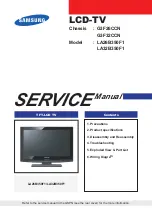
SERVICE MANUAL

20

"

 COLOR LCD TELEVISION

LCD-B20B6

LCD-B20A6

Summary of Contents for LCD-B20A6

Page 1: ...SERVICE MANUAL 20 COLOR LCD TELEVISION LCD B20B6 LCD B20A6...

Page 2: ...ision 5 1 Electrical Adjustment Instructions 6 1 Block Diagrams 7 1 Schematic Diagrams CBA s and Test Points 8 1 Waveforms 9 1 Wiring Diagram 10 1 Exploded View 11 1 Mechanical Parts List 12 1 Electri...

Page 3: ...BG I DK Sound PAL BG PAL I PAL DK MHz MHz MHz MHz 38 9 33 4 32 9 32 4 2 Video S N White 50 CH 3 dB 45 40 3 Audio S N Output Level 500mV dB 53 47 Description Condition Unit Nominal Limit 1 Number of P...

Page 4: ...terminal screw and if applicable to the coaxial connector If the measured resistance is less than 1 0 megohm or greater than 5 2 megohm an abnormality exists that must be corrected before the instrum...

Page 5: ...near thermally hot parts be sure that leads and components do not touch thermally hot parts c the AC supply d high voltage and e antenna wiring Always inspect in all areas for pinched out of place or...

Page 6: ...s H When a power cord has been replaced check that 5 6 kg of force in any direction will not loosen it I Also check areas surrounding repaired locations J Use care that foreign objects screws solder d...

Page 7: ...prongs and externally exposed accessible parts RF terminals an tenna terminals video and audio input and output ter minals microphone jacks earphone jacks etc Measuring Method Power ON Insert load Z...

Page 8: ...the flat pack IC is fixed with glue to the CBA when removing entire flat pack IC first apply soldering iron to center of the flat pack IC and heat up Then remove glue will be melted Fig S 1 6 4 Relea...

Page 9: ...ins of the flat pack IC you can remove it easily Fig S 1 3 2 Affix the wire to a workbench or solid mounting point as shown in Fig S 1 5 3 While heating the pins using a fine tip soldering iron or hot...

Page 10: ...ur due to a potential difference caused by electrostatic charge during unpacking or repair work 1 Ground for Human Body Be sure to wear a grounding band 1 M that is properly grounded to remove any sta...

Page 11: ...bs L 2 5 Refer to the following Reference Notes in the Table Step Loc No Part Removal Fig No Remove Unhook Unlock Release Unplug Unclamp Desolder Note 1 Tilt Stand Assembly D1 4 S 1 2 Rear Cabinet D1...

Page 12: ...D2 S 12 Speaker Holders S 11 S 11 S 6 S 5 10 IR Sensor CBA 3 Jack Holder 8 Function CBA 9 Speaker 11 Front Cabinet Speaker Holders S 6 4 Inverter CBA 5 Main CBA 9 Speaker S 10 S 4 S 4 S 7 S 7 S 7 S 9...

Page 13: ...4 3 L4630DC Fig D3 S 13 S 13 S 14 12 Stand Cover 13 Arm Holder 14 Sheet L 15 Arm Assembly 14 Sheet R...

Page 14: ...BA CN310 To Speaker Function CBA CN801 To Speaker CLN53 CN101A CN102A CN103A CN101B CN102B CN103B Main CBA CN404 CN304 Inverter CBA CN301 CN302 CN303 CN53 CN106 CN31B CN311 CN312 LCD Main CBA Unit To...

Page 15: ...ion 1 Turn the power on Use main power on the TV unit 2 To enter the service mode press STANDBY 2 7 1 and MUTE buttons on the remote control unit in that order within 5 seconds To cancel the service m...

Page 16: ...ss STANDBY button on the remote control 1 Initial Setting General Enter the Service mode Set the each initial data as shown on table 1 below Table 1 Initial Data ITEM BUTTON on the remote control DATA...

Page 17: ...SC 143 BRIGHT 0 0 NORMAL 0 65 DARK 0 98 COR C D S 1 VOL p 1 128 COG C D S 1 VOL p 2 128 COB C D S 1 VOL p 3 128 DR C D S 1 VOL p 4 180 DG C D S 1 VOL p 5 180 DB C D S 1 VOL p 6 180 SBR C D S 1 VOL p 7...

Page 18: ...thin specification adjust DB C D S 1 or DR C D S 1 Refer to 1 Initial Setting RF AV2 CVBS APL 40 Press 3 button to select COB C D S 1 for Blue adjustment Press 1 button to select COR C D S 1 for Red a...

Page 19: ...CL 6 SDA 5 7 WP AL 5V AL 5V CN105 IS USED FOR ADJUSTMENT AT FACTORY MPWEL MPCE MPOE MPSEL 0 MPWEH RESET QH HDIN FBIN BUS OPEN 2 DVP RESET PC 8 DVP CLK PC 5 CN301 NO CONNECTION DVP SOUT PC 6 DVP SIN PC...

Page 20: ...BLOCK DIAGRAM C Y TO LCD BLOCK DIAGRAM CN103B IC781 INPUT SELECT SW CONTROL 10 9 11 INPUT 0 INPUT 1 TO SYSTEM CONTROL BLOCK DIAGRAM Q872 Q871 TUNER UNIT BUFFER WF7 WF2 WF3 WF6 WF5 WF4 3 5 4 12 13 14...

Page 21: ...IN JK723 SIF JK724 AUDIO1 R IN 14 IC801 AUDIO AMP 7 VOLUME 11 AMP AMP MUTE STANDBY CONTROL 6 1 R CH L CH 2 JK801 HEADPHONE JACK CN801 SP R 1 GND 2 TO IF VIDEO BLOCK DIAGRAM 3 15 WF1 CLN801 SP801 SPEA...

Page 22: ...2 OR 3 31 OR 4 30 OR 5 29 OR 0 34 OR 1 33 OR 2 32 OG 3 24 OG 4 23 OG 5 22 OG 0 27 OG 1 26 OG 2 25 OB 3 17 OB 4 16 OB 5 15 OB 0 20 OB 1 19 OB 2 18 ER 3 3 ER 4 2 ER 5 1 ER 0 6 ER 1 5 ER 2 4 EG 3 47 EG 4...

Page 23: ...AL 40V TO SYSTEM CONTROL BLOCK DIAGRAM TO INVERTER BLOCK DIAGRAM F601 T4A L 250V Q608 Q603 Q504 Q633 Q502 Q632 Q507 Q506 6V REG 5V REG IC602 3 3V REG IC605 5V REG 5V REG Q501 25V REG Q503 10 8V REG Q5...

Page 24: ...9 7 3 5 2 6 1 4 10 8 TO POWER SUPPLY BLOCK DIAGRAM TO SYSTEM CONTROL BLOCK DIAGRAM MAIN CBA 22V 7 7 CN404 CN304 22V 6 6 22V 5 5 22V 4 4 22V 8 8 22V 9 9 CURRENT CONTROL SWITCH Q341 Q344 T302 OVER VOLTA...

Page 25: ...ings for ordering The correct part number is shown in the parts list and may be slightly different or amended since these drawings were prepared 2 All resistance values are indicated in ohms K 103 M 1...

Page 26: ...d 2 To maintain original function and reliability of repaired units use only original replacement parts which are listed with their part numbers in the parts list section of the service manual 4 Volta...

Page 27: ...8 3 L4630SCM1 Main 1 4 Schematic Diagram...

Page 28: ...30SCM2 Main 2 4 Schematic Diagram CN103A 1 0 1 2 0 4 3 0 2 4 0 5 2 6 6 2 6 7 0 8 1 7 9 0 2 10 0 11 3 5 12 5 2 13 6 9 14 3 1 15 0 16 4 8 17 0 18 5 2 19 0 20 5 2 21 3 3 22 3 1 23 0 VOLTAGE CHART Pin No...

Page 29: ...If Main Fuse F601 is blown check to see that all components in the power supply circuit are not defective before you connect the AC plug to the AC power supply Otherwise it may cause some components i...

Page 30: ...CM4 Main 4 4 IR Sensor Schematic Diagram CN102A 1 3 8 2 0 3 0 1 4 5 2 5 5 2 6 3 3 7 0 2 8 0 9 2 0 10 0 11 4 4 12 0 4 13 3 8 14 1 5 15 3 4 16 0 17 0 18 5 2 19 5 2 20 0 21 0 22 0 23 0 VOLTAGE CHART Pin...

Page 31: ...8 7 Function Schematic Diagram L4630SCF...

Page 32: ...8 8 L4630SCINV Inverter Schematic Diagram...

Page 33: ...8 9 L4630SCL1 LCD Main 1 2 Schematic Diagram...

Page 34: ...8 10 L4630SCL2 LCD Main 2 2 Schematic Diagram...

Page 35: ...nit If Main Fuse F601 is blown check to see that all components in the power supply circuit are not defective before you connect the AC plug to the AC power supply Otherwise it may cause some componen...

Page 36: ...e a hot chassis ground is present in the power supply circut an isolation transformer must be used Also in order to have the ability to increase the input slowly when troubleshooting this type power s...

Page 37: ...8 13 IR Sensor CBA Top Bottom View Function CBA Top View Function CBA Bottom View BL4520F01011 2 BL4520F01011 3...

Page 38: ...8 14 Inverter CBA Top View Inverter CBA Bottom View BL2500F01021...

Page 39: ...ck points Shown in Schematic Diagram WF1 Pin 14 of IC801 AUDIO 0 1V 0 5ms WF2 Pin 1 of IC781 S VIDEO Y 0 2V 10 s WF3 Pin 13 of IC781 S VIDEO C 0 2V 20 s WF4 Pin 3 of CN103A B 0 5V 5 s WF7 Pin 9 of CN1...

Page 40: ...ith 1kHz Audio Signal WF9 WF14 Waveforms to be observed at Waveform check points Shown in Schematic Diagram WF9 R997 WF10 R902 WF11 R901 WF12 R904 WF13 R907 WF14 R905 CTKH 1V 20ns STH1 1V 1 s POL 1V 2...

Page 41: ...5 20 18 16 14 12 6 8 11 10 9 7 5 1 3 4 2 AC601 AC CORD CN312 1 GND 2 NU 3 VCOM 4 VCOM 5 TEST 6 PANEL 25V 7 TEST 8 PANEL 3 3V 9 NU 10 PANEL 6V 11 NU 12 OFFEV 13 STV1 14 CLKV 15 NU 16 GND 17 NU 18 NU 19...

Page 42: ...21 L21 L21 L16 L21 L9 L9 L9 L9 L9 A4 B5 B5 B3 B34 B18 B18 B18 B18 L23 S5 L17 L27 L22 L4 B14 L4 L4 A7 A3 L4 B5 B5 B14 B14 B5 B5 CLN801 SP801 CLN310 SP802 See Electrical Parts List for parts with this m...

Page 43: ...L21 L16 L21 L9 L9 L9 L9 L9 A4 B5 B5 B3 B34 B18 B18 B18 B18 L23 S5 L17 L27 L22 L4 B14 L4 L4 A7 A3 L4 B5 B5 B14 B14 B5 B5 CLN801 SP801 CLN310 SP802 See Electrical Parts List for parts with this mark Ma...

Page 44: ...11 3 L4630_31PEX Packing S1 FRONT S2 S5 S4 Tape Packing Tape Packing Tape Packing Tape Packing Tape S3 X1 Some Ref Numbers are not in sequence X5 X3 X2 1...

Page 45: ...STAND HOLDER L3253UD 1EM321693 B13 CLOTH 15X10XT0 5 L9700UA 0EM405038 B14 A SPEAKER HOLDER L4630BA 1EM423840 B14 B SPEAKER HOLDER L4620EA 1EM423593 B17 WASHER 10X5XT0 5 L4620EA 1EM423834 B18 CLOTH 10X...

Page 46: ...01 F 50V CHD1JK30B103 C512 CHIP CERAMIC CAP 1608 B K 0 01 F 50V CHD1JK30B103 C513 ELECTROLYTIC CAP 220 F 6 3V M H7 or CE0KMAVSL221 ALUMINUM ELECTROLYTIC CAP 220 F 6 3V H7 CE0KMAVSM221 C517 ELECTROLYT...

Page 47: ...E1CMASTM470 Ref No Description Part No C743 CHIP CERAMIC CAP F Z 2 2 F 10V CHD1AZ30F225 C745 ELECTROLYTIC CAP 47 F 16V M or CE1CMASDL470 ELECTROLYTIC CAP 47 F 16V M or CA1C470SP085 ALUMINUM ELECTROLYT...

Page 48: ...DIODE 1SS400 or QD1Z001SS400 SWITCHING DIODE KDS160E RTK P ND1ZKDS160EP D403 ZENER DIODE MTZJT 7718B or QDTB00MTZJ18 ZENER DIODE DZ 18BSBT265 NDTB00DZ18BS D404 SWITCHING DIODE 1SS400 or QD1Z001SS400...

Page 49: ...or NSZBA0SJY041 VOLTAGE REGULATOR KA7805A NSZBA0SF3052 IC781 IC SWITCH TC4053BF EL N F QSZBA0TTS163 IC801 IC AN17812A QSZBA0SMS017 IC831 IC AUDIO PROCESSOR MSP3417G QG B8 V3 NSZBA0SP3005 Ref No Descr...

Page 50: ...J 10k RCX4JATZ0103 R518 CHIP RES 1 10W J 10k or RRXAJR5Z0103 Ref No Description Part No RES CHIP 1608 1 10W J 10k RRXA103YF002 R519 CARBON RES 1 4W J 150 RCX4JATZ0151 R520 CHIP RES 1 10W J 56k or RRXA...

Page 51: ...RRXAZR5Z0000 RES CHIP 1608 1 10W J 0 RRXA000YF002 R737 CHIP RES 1 10W J 1k or RRXAJR5Z0102 Ref No Description Part No RES CHIP 1608 1 10W J 1 0k RRXA102YF002 R738 CHIP RES 1 10W J 1k or RRXAJR5Z0102...

Page 52: ...J 22k or RRXAJR5Z0223 RES CHIP 1608 1 10W J 22k RRXA223YF002 R884 CHIP RES 1 10W J 22k or RRXAJR5Z0223 Ref No Description Part No RES CHIP 1608 1 10W J 22k RRXA223YF002 R885 CHIP RES 1 10W J 22k or R...

Page 53: ...LECTROLYTIC CAP 220 F 16V M or CA1C221SP085 ELECTROLYTIC CAP 220 F 16V M CE1CMASTM221 C321 CAP CHIP 5pF 3KV C XC CA3F5R05M016 C322 CHIP CERAMIC CAP 1608 B K 0 01 F 50V CHD1JK30B103 C323 CAP CHIP 5pF 3...

Page 54: ...P NQS4KTC3198P Q305 TRANSISTOR 2SA1175 F or QQSF02SA1175 TRANSISTOR KTA1267 GR AT P or NQS1KTA1267P TRANSISTOR KTA 1266 GR AT P or NQS4KTA1266P TRANSISTOR 2SA1318 T AANP or 2SA1318TZ Ref No Descriptio...

Page 55: ...W J 4 7k or RRXAJR5Z0472 RES CHIP 1608 1 10W J 4 7k RRXA472YF002 R350 CHIP RES 1 10W J 4 7k or RRXAJR5Z0472 RES CHIP 1608 1 10W J 4 7k RRXA472YF002 R351 CHIP RES 1 10W J 10k or RRXAJR5Z0103 RES CHIP 1...

Page 56: ...LCD B20A6 LCD B20B6 L4630BA 31BB 2006 07 28...

Reviews: