background image

2-30


X8STi/X8STi-F/X8STi-3F/X8STi-LN4 User's Manual

LSI 1068E

NIC4 LED

JBMC1

CMOS Clear

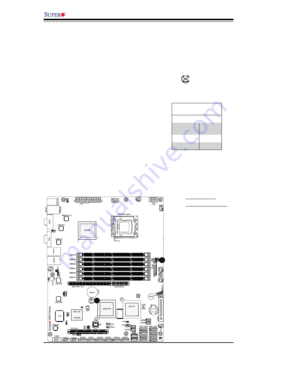
JBT1 is used to clear CMOS. Instead of pins, this "jumper" consists of contact pads 
to prevent accidental clearing of CMOS.  To clear CMOS, use a metal object such 
as a small screwdriver to touch both pads at the same time to short the connection.  
Always remove the AC power cord from the system before clearing CMOS.

Note:

 For an ATX power supply, you must completely shut down the system, remove 

the AC power cord and then short JBT1 to clear CMOS.

A

A. Clear CMOS
B. Watch Dog Enable

Watch Dog Enable/Disable

Watch  Dog  is  a  system  monitor  that  can 
reboot the system when a software appli-
cation hangs. Close pins 1-2 to reset the 
system if an application hangs. Close pins 
2-3  to  generate  a  non-maskable  interrupt 
signal for the application that hangs. See 
the table on the right for jumper settings. 
Watch  Dog  must  also  be  enabled  in  the 
BIOS.  


Watch Dog 

Jumper Settings (JWD)

Jumper Setting     Definition     

Pins 1-2

Reset 

(default)

Pins 2-3

NMI

Open

Disabled

B

Summary of Contents for X8STi

Page 1: ...USER S MANUAL Revision 1 1b X8STi F X8STi 3F X8STi X8STi LN4...

Page 2: ...UCH DAMAGES IN PARTICULAR SUPER MICRO COMPUTER INC SHALL NOT HAVE LIABILITY FOR ANY HARDWARE SOFTWARE OR DATA STORED OR USED WITH THE PRODUCT INCLUDING THE COSTS OF REPAIRING REPLACING INTEGRATING INS...

Page 3: ...tforms Please refer to our web site http www supermicro com products for updates on supported processors This product is intended to be installed and serviced by professional technicians Manual Organi...

Page 4: ...to the components or injury to yourself Danger Caution Instructions to be strictly followed to prevent catastrophic system failure or to avoid bodily injury Warning Important information given to ensu...

Page 5: ...Micro Computer B V Het Sterrenbeeld 28 5215 ML s Hertogenbosch The Netherlands Tel 31 0 73 6400390 Fax 31 0 73 6416525 Email sales supermicro nl General Information support supermicro nl Technical Su...

Page 6: ...D and Control 1 12 1 4 Power Configuration Settings 1 12 Slow Blinking LED for Suspend State Indicator 1 13 BIOS Support for USB Keyboard 1 13 Main Switch Override Mechanism 1 13 Wake On LAN WOL 1 13...

Page 7: ...19 Reset Button 2 20 Power Button 2 20 2 6 Connecting Cables 2 21 ATX Main PWR CPU PWR Connectors 2 21 Fan Headers 2 22 Chassis Intrusion 2 22 Internal Buzzer 2 23 Speaker 2 23 Overheat Fan Fail LED 2...

Page 8: ...Procedures 3 1 3 2 Technical Support Procedures 3 2 3 3 Frequently Asked Questions 3 3 3 4 Returning Merchandise for Service 3 4 Chapter 4 BIOS 4 1 Introduction 4 1 4 2 Main Setup 4 2 4 3 Advanced Set...

Page 9: ...ghest standards in quality and performance Please check that the following items have all been included with your motherboard If anything listed here is damaged or missing contact your retailer The fo...

Page 10: ...rboard X8STi 3F Image Note All graphics shown in this manual were based upon the latest PCB Revision available at the time of publishing of the manual The motherboard you ve received may or may not lo...

Page 11: ...nel connections indicates the location of Pin 1 Jumpers not indicated are for testing only JBMC1 is reserved for internal testing only Do not change the jumper setting pre set by the manufacturer When...

Page 12: ...s 1 2 Default Note Below JBT1 CMOS Clear See Chpt 2 JI2 C1 JI2 C2 SMB to PCI Slots See Chpt 2 JPG1 Onboard VGA Enable Pins 1 2 Enabled JPL1 JPL2 LAN 1 2 Enable Pins 1 2 Enabled JPL3 JPL4 LAN 3 4 Enabl...

Page 13: ...ED Power LED Indicator header JOH Overheat LED header JPW1 24 pin ATX main power connector required JPW2 12V 8 pin CPU power connector required JPWF Power Fail indication header JWOL Wake On LAN heade...

Page 14: ...SAS Activity X8STi 3F only Green Blinking SAS Active LES2 SAS Heartbeat X8STi 3F only Yellow Blinking SAS Normal Differences between Main Features of the X8STi X8STi F X8STi 3F X8STi LN4 Models X8STi...

Page 15: ...pset Intel ICH10R Expansion Slots One 1 PCI Express x16 Gen2 PCI Express x8 in x4 slot One 1 32 bit PCI 33MHz slot Slot 1 Integrated Graphics Matrox G200ew with 8 MB Video Memory Network Connections T...

Page 16: ...http www supermicro com support manuals Integrated IPMI 2 0 for the X8STi F X8STi 3F only IPMI 2 0 supported by the WPCM450 Server BMC Note For IPMI Configuration Instructions please refer to the Embe...

Page 17: ...D and control CPU Thermal Trip support Thermal Monitor 2 TM2 support Fan Control Fan status monitoring with firmware 4 pin Pulse Width Modulation fan speed control Low noise fan speed control System M...

Page 18: ...PCI E Gen2 x16 X58 W83627DHG COM1 COM2 Floppy Keyboard Mouse SPI SPI BIOS ICH10R LPC I O DMI Intel 82574L PCIE_x1 RJ45 SATAII 3 0G USB x 8 SATA x6 USB2 0 DDR3 1333 1066 800 LGA1366_Socket CPU DIMM_CHB...

Page 19: ...I technology built in the X8STi X8STi F X8STi 3F X8STi LN4 is one of the first motherboards on the market that offers the next generation point to point system interconnect interface replacing the cur...

Page 20: ...an the following voltages continuously CPU Core Chipset Voltage Memory Voltage 1 8V 3 3V 3 3V standby 5V 5V Standby Vbat and 12V Once a voltage becomes unstable it will give a warning or send an error...

Page 21: ...to turn off the power just press and hold the power button for 4 seconds The power will turn off and no power will be provided to the motherboard Wake On LAN WOL Wake On LAN is defined as the ability...

Page 22: ...K 1 2 M 1 44 M or 2 88 M disk drives and data transfer rates of 250 Kb s 500 Kb s or 1 Mb s It also provides two high speed 16550 compatible serial communication ports UARTs Each UART includes a 16 b...

Page 23: ...rpose I O 3SGPIO ports The WPCM450 also includes the following features One X Bus parallel interface for expansion I O connections Three ADC inputs Analog and Digital Video outputs Two serial for boun...

Page 24: ...1 16 X8STi X8STi F X8STi 3F X8STi LN4 User s Manual Notes...

Page 25: ...its edges only do not touch its components peripheral chips memory modules or gold contacts When handling chips or modules avoid touching their pins Put the motherboard and peripherals back into their...

Page 26: ...nk and heatsink fans When purchasing an LGA 1366 processor or when receiving a motherboard 4 with an LGA 1366 processor pre installed make sure that the CPU plastic cap is in place and none of the CPU...

Page 27: ...cket or its pins to avoid damaging the CPU or the socket With the CPU inside the socket in 7 spect the four corners of the CPU to make sure that the CPU is properly installed Once the CPU is securely...

Page 28: ...before installing the heatsink To install the heatsink bracket please insert four screws to the mounting holes to secure the bracket on the motherboard If you do not use a screw_type heatsink please...

Page 29: ...3 remove the heatsink screws from the motherboard in the se quence as show in the picture on the right Hold the heatsink as shown 4 in the picture on the right and gently wriggle the heatsink to loose...

Page 30: ...oles Please take all necessary precautionary measures to avoid damaging these compo nents when installing the motherboard into the chassis Tools Needed Philips Screwdriver 9 Pan head 6 screws Installa...

Page 31: ...d number of DIMMs into the memory 1 slots starting with DIMM1A When populating multiple DIMM modules within a channel always start with blue slot first For best performance please use the memory modul...

Page 32: ...is used The reduction in memory availability is disproportional DIMM3B DIMM2A DIMM2B DIMM1A DIMM1B DIMM3A Memory Support The X8STi X8STi F X8STi 3F X8STi LN4 supports up to 24 GB Unbuffered ECC or No...

Page 33: ...emory System BIOS 1 MB 3 99 GB Local APIC 4 KB 3 99 GB Area Reserved for the chipset 2 MB 3 99 GB I O APIC 4 Kbytes 4 KB 3 99 GB PCI Enumeration Area 1 256 MB 3 76 GB PCI Express 256 MB 256 MB 3 51 GB...

Page 34: ...ation See the figure below for the colors and locations of the various I O ports Back Panel Connectors and IO Ports Back Panel Connectors 1 Keyboard Purple 7 VGA 2 PS 2 Mouse Green 8 LAN1 3 USB Port 0...

Page 35: ...the table at right for pin definitions PS 2 Keyboard Mouse Pin Definitions PS2 Keyboard PS2 Mouse Pin Definition Pin Definition 1 KB Data 1 Mouse Data 2 No Connection 2 No Connection 3 Ground 3 Ground...

Page 36: ...ons USB 2 3 USB 4 5 USB 6 and USB 7 are used to provide front chassis access USB 6 and USB 7 are Type A Connec tors USB Cables are not included See the tables on the right for pin definitions Back Pan...

Page 37: ...hese ports accept RJ45 type cables Notes 1 The IPMI Dedicated LAN is for the X8STi F X8STi 3F only LAN3 and LAN4 are for X8STi LN4 only 2 Please refer to the LED Indicator Section for LAN LED informat...

Page 38: ...ted on the IO Backplane and a Serial port is lo cated next to FP USB 2 3 to provide front access See the table on the right for pin definitions Serial Port Pin Definitions COM1 COM2 Pin Definition Pin...

Page 39: ...llation 2 15 1 VGA Video Connector A Video VGA connector is located next to the COM Port on the IO backplane This connector is used to provide video and CRT display Refer to the board layout below for...

Page 40: ...ically for use with Supermicro server chassis See the figure below for the descriptions of the various control panel buttons and LED indicators Refer to the following section for descriptions and pin...

Page 41: ...header is located on pins 19 and 20 of JF1 Refer to the table on the right for pin definitions Power Button OH Fan Fail LED 1 NIC1 LED Reset Button 2 Power Fail LED HDD LED Power LED 3 4 1 2 Vcc Vcc...

Page 42: ...NIC3_LED and NIC4_LED to display network activities for LAN 3 and LAN4 Refer to the table on the right for pin definitions HDD LED UID Switch The HDD LED and UID Switch con nections are located on pi...

Page 43: ...blue UID signals or to provide advanced warn ings for chassis overheat fan failure Refer to the table on the right for pin definitions Power Fail LED The Power Fail LED connection is located on pins...

Page 44: ...le on the right for pin definitions Power Button Pin Definitions JF1 Pin Definition 1 Signal 2 3V Standby Reset Button The Reset Button connection is located on pins 3 and 4 of JF1 Attach it to a hard...

Page 45: ...Power 24 pin Connector Pin Definitions JPW1 Pin Definition Pin Definition 13 3 3V 1 3 3V 14 12V 2 3 3V 15 COM 3 COM 16 PS_ON 4 5V 17 COM 5 COM 18 COM 6 5V 19 COM 7 COM 20 Res NC 8 PWR_OK 21 5V 9 5VSB...

Page 46: ...omatically set fan speeds based on the system temperature The default setting is Disabled which allows the onboard fans to run at full speed Refer to the table on the right for pin definitions A B A F...

Page 47: ...uzzer A Internal Buzzer B Speaker Internal Buzzer Pin Definition Pin Definitions Pin 1 Pos Beep In Pin 2 Neg Alarm Speaker Speaker On the JD1 header Pins 3 4 are used for internal speaker Close Pins 3...

Page 48: ...on 1 5vDC 2 OH Active OH Fan Fail LED Status State Message Solid Overheat Blinking Fan Fail A B NIC3_LED NIC4_LED X8STi LN4 Only NIC3_LED and NIC4_LED headers provide LAN3 LAN4 Activity LED connection...

Page 49: ...table on the right for pin definitions PWR Supply I2 C Pin Definitions Pin Definition 1 Clock 2 Data 3 PWR Fail 4 Ground 5 3 3V Onboard Power LED An onboard Power LED header is located at JLED This P...

Page 50: ...ers are used to communicate with the enclosure management chip in the system See the table on the right for pin definitions Refer to the board layout below for the locations of the headers NC No Conne...

Page 51: ...n X8STi 3F only A B I Button X8STi 3F only An onboard I Button located next to the floppy drive is an 1 wire computer chip enclosed in a durable stainless steel can I Button stores instructions provid...

Page 52: ...R Supply Fail LED Pin Definitions Pin Definition 1 PWR 1 Fail 2 PWR 2 Fail 3 PWR 3 Fail 4 Signal Alarm Reset Unit Identifier Switches There are two Unit Identifier UID Switches on the motherboard The...

Page 53: ...t board Note On two pin jumpers Closed means the jumper is on and Open means the jumper is off the pins A A LAN Port 1 Enable B LAN Port 2 Enable C LAN Port 3 Enable X8STi LN4 D LAN Port 4 Enable X8ST...

Page 54: ...power supply you must completely shut down the system remove the AC power cord and then short JBT1 to clear CMOS A A Clear CMOS B Watch Dog Enable Watch Dog Enable Disable Watch Dog is a system monit...

Page 55: ...1 Both Jumpers Definition Pins 1 2 Enabled Pins 2 3 Disabled VGA Enable JPG1 allows you to enable or disable the onboard VGA connector The default position is on pins 1 and 2 to enable VGA See the tab...

Page 56: ...ht for jumper settings and jumper connections Note JPUSB1 is used for Backpanel USB ports 0 1 JPUSB2 is for Front Panel USB ports 2 3 and 4 5 JPUSB3 is used for Front Accessible USB Ports 6 and 7 When...

Page 57: ...osition is on pins 1 and 2 to enable SAS See the table on the right for jumper settings SAS RAID Mode Select Jumper Settings Settings Definition Close Software RAID Enabled Default Open IT Mode Enable...

Page 58: ...Definition Pins 1 2 Default Note Do not change the manufacturer s default setting JBMC1 X8STi F X8STi 3F Only Note JBMC1 BMC Jumper is reserved for internal testing only Do not change the jumper sett...

Page 59: ...r Definition Off No Connection or 10 Mbps Green 100 Mbps Amber 1 Gbps LAN 1 LAN 2 LAN 3 LAN 4 Activity LEDs Yellow Color Status Definition Yellow Blinking Active Rear View Activity LED Link LED C B IP...

Page 60: ...ails Also see the layout below for the LED location SAS Heartbeat LED Indicator LE5 LED Settings Blinking Yellow SAS is ready for use SAS Activity LED X8STi 3F Only A SAS Activity LED is located at LE...

Page 61: ...e is connected Make sure to disconnect the power cable before removing or installing any component See the layout below for the LED location A A Onboard PWR LED B BMC Heartbeat LED BMC Heartbeat LED A...

Page 62: ...al UID LED The Unit Identifier LED Indicator is located at LE2 on the motherboard When the blue light is on the unit system that might be in need of service is identified See the layout below for the...

Page 63: ...located on the motherboard In addition to six SATA ports eight SAS con nections are also located on the X8STi 3F These Serial Link connections provide faster data transmission than the connections of...

Page 64: ...Ground 16 Motor Enable 17 Ground 18 DIR 19 Ground 20 STEP 21 Ground 22 Write Data 23 Ground 24 Write Gate 25 Ground 26 Track 00 27 Ground 28 Write Protect 29 Ground 30 Read Data 31 Ground 32 Side 1 S...

Page 65: ...motherboard and chas sis 3 Disconnect all ribbon wire cables from the motherboard including those for the keyboard and mouse Also be sure to remove all add on cards 4 Install a CPU and heatsink be sur...

Page 66: ...poor quality power supply may cause the system to lose the CMOS setup information Refer to Section 1 5 for details on recommended power supplies 2 The battery on your motherboard may be old Check to v...

Page 67: ...mail at support supermicro com by phone at 408 503 8000 option 2 or by fax at 408 503 8019 3 3 Frequently Asked Questions Question What type of memory does my motherboard support Answer The X8STi X8ST...

Page 68: ...eted your system will automatically reboot If you choose the exe file please run the exe file under Windows to create the BIOS flash floppy disk Insert the floppy disk into the system you wish to flas...

Page 69: ...ly or wait 4 seconds before powering down Answer Enter the BIOS Setup Advanced Boot Feature Power Button Function Select Instant Off if you want the system to power down instantly when the power butto...

Page 70: ...3 6 X8STi X8STi F X8STi 3F X8STi LN4 User s Manual Notes...

Page 71: ...options cannot be configured Options in blue can be configured by the user The right frame displays the key legend Above the key legend is an area reserved for a text message When an option is select...

Page 72: ...ng Do not upgrade the BIOS unless your system has a BIOS related issue Flashing the wrong BIOS can cause irreparable damage to the system In no event shall Supermicro be liable for direct indirect spe...

Page 73: ...to move between fields The date must be entered in Day MM DD YY format The time is entered in HH MM SS format Note The time is in the 24 hour format For example 5 30 P M appears as 17 30 00 Supermicro...

Page 74: ...s the bootup screen options to be modified between POST mes sages or the OEM logo Select Disabled to display the POST messages Select Enabled to display the OEM logo instead of the normal POST message...

Page 75: ...on after a power loss Select Last State to allow the system to resume its last state before a power loss The options are Power On Power Off and Last State Interrupt 19 Capture Interrupt 19 is the sof...

Page 76: ...method of ordering for the Multiple APIC Description Table MADT Select Modern Ordering for Microsoft Windows XP or later Select Legacy Order ing for Microsoft Windows 2000 or earlier The options are...

Page 77: ...in an effort to reduce power consump tion and heat dissipation Please refer to Intel s web site for detailed information The options are Disable Disable GV3 and Enable Enable GV3 Intel Turbo Boost Con...

Page 78: ...e package limit setting If set to Auto the AMI BIOS will automatically set the limit on the C State package register The options are Auto C1 C3 C6 and C7 C1 Auto Demotion When enabled the CPU will con...

Page 79: ...se this option to set the QPI frequency The options are Auto 4 800 GT 5 866 GT and 6 400 GT QPI L0s and L1 QuickPath Interconnect QPI offers three power states called L0 L0s and L1 L0 is a normal oper...

Page 80: ...d as well Select Enabled to use Demand Scrub bing for ECC memory correction The options are Enabled and Disabled Patrol Scrubbing Patrol Scrubbing is a process that allows the CPU to correct correctab...

Page 81: ...to send debug information to The options are Disabled PCI and LPC Extend PCI Hole Select Enabled when using a 64 bit Operating System The options are Disabled and Enabled USB Functions This feature a...

Page 82: ...E is enabled under Configure SATA 1 as above Selecting Enhanced will set SATA 2 to native SATA mode The options are Disabled Enhanced IDE Detect Timeout sec Use this feature to set the time out value...

Page 83: ...ses The options are Auto 0 1 2 3 and 4 Select Auto to allow the AMI BIOS to automatically detect the PIO mode Use this value if the IDE disk drive support cannot be determined Select 0 to allow the AM...

Page 84: ...ata transfer rate of 44 4 MB s Select UDMA4 to allow the BIOS to use Ultra DMA mode 4 It has a data transfer rate of 66 7 MB s Select UDMA5 to allow the BIOS to use Ultra DMA mode 5 It has a data tran...

Page 85: ...The options are Disabled and Enabled PCIE I O Performance This feature selects the setting for the IOH PCIE maximum payload size The op tions are 128B and 256B Slot 6 Width This feature selects the bu...

Page 86: ...lable Select 3F8 IRQ4 to allow the serial port to use 3F8 as its I O port address and IRQ 4 for the interrupt address The options for Serial Port1 are Disabled 3F8 IRQ4 2E8 IRQ3 The options for Serial...

Page 87: ...sabled Sredir Memory Display Delay This feature defines the length of time in seconds to display memory information The options are No Delay Delay 1 Sec Delay 2 Sec and Delay 4 Sec Hardware Health Con...

Page 88: ...d Medium The processor is running warmer This is a precautionary level and generally means that there may be factors contributing to this condition but the CPU is still within its normal operating sta...

Page 89: ...ng CPU Fan speed triggering the Overheat Alarm etc Since CPUs can have different Tem perature Tolerances the installed CPU can now send its Temperature Toler ance to the motherboard resulting in bette...

Page 90: ...PWM Cycle Performance PF 70 of PWM Cycle Balanced BL 50 of PWM Cycle and Energy Saving ES 30 of PWM Cycle Voltage Reading This feature displays the current voltage detected of the various components...

Page 91: ...erfaces that IT administrators can use to monitor system health and to manage the system as a whole For more information on the IPMI specifications please visit Intel s website at www intel com IPMI F...

Page 92: ...P address for this machine This should be in decimal and in dotted quad form i e 192 168 10 253 The value of each three digit number separated by dots should not exceed 255 Subnet Mask Subnet masks te...

Page 93: ...tions are OK and Cancel Clear event log This option clears the Event Log memory of all messages The options are OK and Cancel PCIE Error Log Use this option to enable logging of errors encountered in...

Page 94: ...such a password has not been used and Set means a user password has been entered for the system Change Supervisor Password Select this feature and press Enter to access the submenu and then type in a...

Page 95: ...y Drive 2nd Boot Device USB XXXXXXXXX 3rd Boot Device SATA XXXXXXXXX 4th Boot Device Network XXXXXXXXX 5th Boot Device Network XXXXXXXXX Clear User Password Available only if User Password has been se...

Page 96: ...ves This feature allows the user to specify the boot sequence from all available hard disk drives The settings are Disabled and a list of all hard disk drives that have been detected i e 1st Drive 2nd...

Page 97: ...to discard all the changes and return to the AMI BIOS Utility Program Load Optimal Defaults To set this feature select Load Optimal Defaults from the Exit menu and press Enter Then select OK to allow...

Page 98: ...4 28 X8STi X8STi F X8STi 3F X8STi LN4 User s Manual Notes...

Page 99: ...al This section lists Beep Codes for recoverable POST errors Recoverable POST Error Beep Codes When a recoverable type of error occurs during POST BIOS will display a POST code that describes the prob...

Page 100: ...A 2 X8STi X8STi F X8STi 3F X8STi LN4 User s Manual Notes...

Page 101: ...ID driver displays When the Windows XP 2003 Setup screen appears press S to specify ad 3 ditional device s Insert the driver diskette Intel AA RAID XP 2003 Driver for ICH10R into 4 Drive A and press t...

Page 102: ...o proceed with the installation process If you need 5 to specify any additional devices to be installed do it at this time Once all devices are specified press the Enter key to continue with the insta...

Page 103: ...each item you must re boot the system before proceeding with the next item on the list The bottom icon with a CD on it allows you to view the entire contents of the CD Appendix C Software Installatio...

Page 104: ...ctor III displays crucial system information such as CPU temperature system voltages and fan status See the Figure below for a display of the Supero Doctor III interface Note 1 Both default user name...

Page 105: ...te Control Note SD III Software Revision 1 0 can be downloaded from our Web site at ftp ftp supermicro com utility Supero_Doctor_III You can also download SDIII User s Guide at http www supermicro com...

Page 106: ...C 4 X8STi X8STi F X8STi 3F X8STi LN4 User s Manual Notes...

Page 107: ...rted at this time Below is a two part procedure to recover the BIOS Part 1 Boot Sector Recovery Process 1 Using a different system download and copy the correct BIOS binary image into a USB flash devi...

Page 108: ...Drive as above except that the BIOS image file super rom is loaded from an IDE ATAPI CD DVD ROM RW disc drive that is attached to the system Note that loading from an IDE SATA hard disk drive is NOT...

Page 109: ...expected to result in significant injury or loss of life or catastrophic property damage Accordingly Supermicro disclaims any and all liability and should buyer use or sell such products for use in su...

Reviews: