


1-8
X7DVL-3/X7DVL-i User's Manual
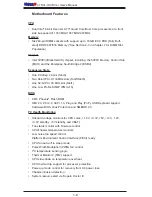
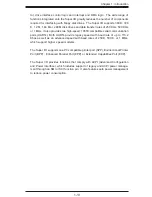
Figure 1-9. Block Diagram of the 5000V Chipset
Note:
This is a general block diagram. Please see the previous Motherboard Features
pages for details on the features of each motherboard.
USB 2.0
3.0 Gb/S
PORT
PORT
PORT
PORT
PORT PORT
PORT
PORT
#0
MCH
PROCESSOR#2
ESB2
PCI 32/33MMZ
GILGAL
GB LAN
FWH
RJ45
RJ45
LPC
COM2
COM1
SIO
W83627
FDD
PCI-X133MHz
PARALLEL
PORT
IDE CONN
ATA 100
KB
MS
VRM
ISL6306
#2,3
#4,5
#6,7
#4
#3
#1,2
#0
VRM
ISL6306
PROCESSOR#1
667/1067/1333
MT/S
667/1067/1333
MT/S
PCI-X SLOT
J13
#5
#2
#2
PCI-EXP X8
J10
#6
PCI-EXP_X8_SLOT
HF
USB
#0
#1
#2
#3
#4
PCIE X8
PCIE X4
FBD CHNL0
FBD CHNL1
#1
#1
#0
#0
FBD DIMM
FBD DIMM
SATA
#0
#1
#2
#3
#4
#5
#5
SIMLP CONN
VGA
XGI Z7
VGA
CONN
LSI
SAS
1068E
PCI-EX4
3.0Gb/S
SAS/SATA
#0
#1#2
#3
#4
#5
#6
#7
PCI32_3.3V_SLOT
J6
#1
PCI-X_SLOT
J12
#6


