background image

1-8

H8DGG-QF Serverboard User’s Manual

AMD

Socket G34

CPU2

HT3 Link

(8+8)x(8+8)-6.4GT/s

HT3 Link
16x16-5.2GT/s

HT3 Link

8x8-3.2GT/s

PCI-E GEN2  X16

Slot3

SATA  x6

PCI-E GEN2 X16

Slot1

A-Link

SP5100

BMC

VGA

WPCM450-R

PCI

LPC

USB

SIO

W83527

HWM

W83795G

SPI Flash

RMII

DDR2 SDRAM

64Mb X16bit

PSU I2C

IPMB

FE PHY

RTL8201N

VGA

Clock Gen

TPM 

(/OPT)

SR5690-S

COM

PCI-E GEN2 X4

INTEL

KAWELA

RJ45

RJ45

SR5690-M

Slot5

Slot2

Slot4

PCI-E GEN2  X8

PCI-E GEN2  X8

PCI-E GEN2 X16

HT3 Link
16x16-5.2GT/s

HT3 Link

8x8-3.2GT/s

AMD

Socket G34

CPU1

DIMM A1

DIMM A0

DIMM B0

DIMM B1

DIMM C0

DIMM C1

DIMM D0

DIMM D1

DIMM A0

DIMM A1

DIMM B0

DIMM B1

DIMM C0

DIMM C1

DIMM D0

DIMM D1

4xUSB

RJ45

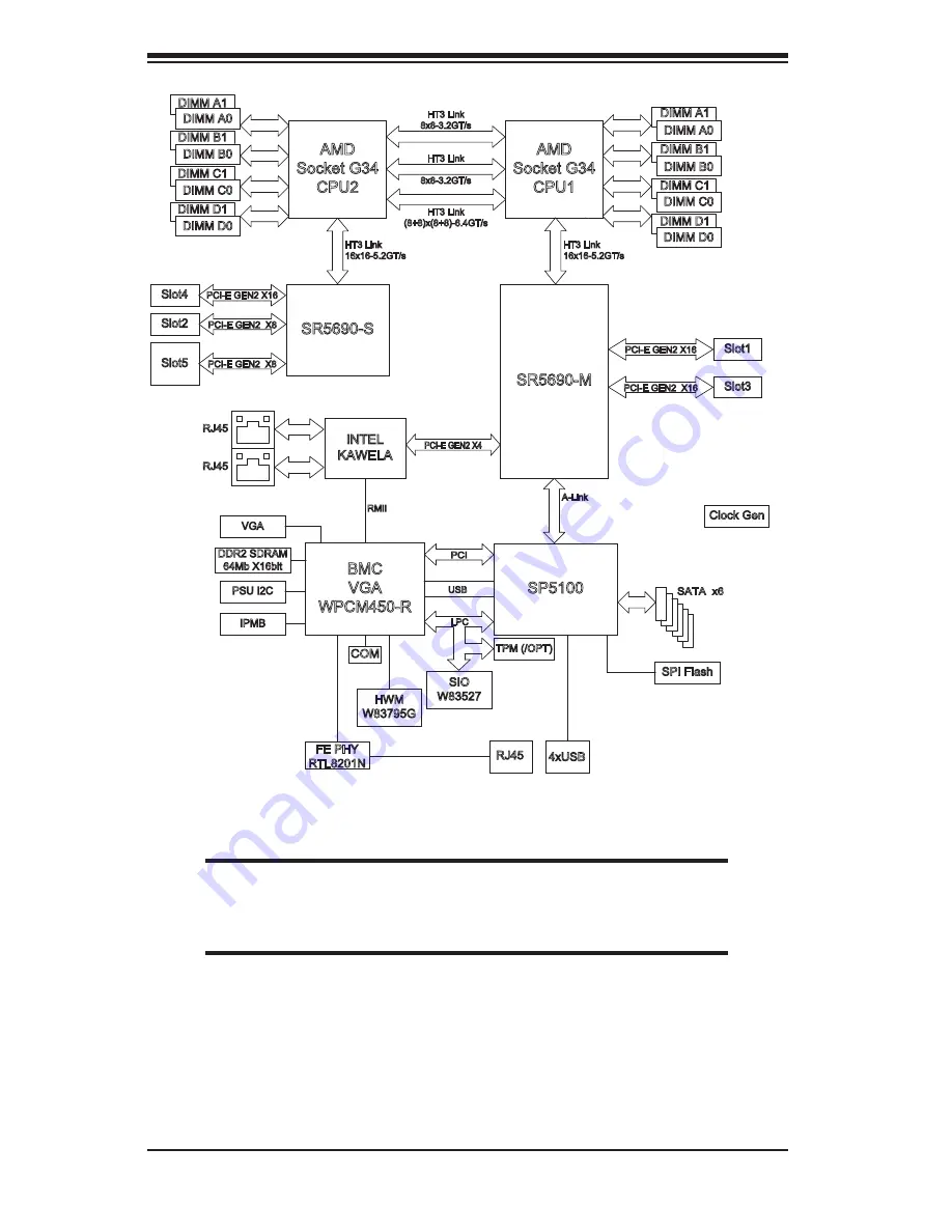
Figure 1-3. AMD SR5690/SP5100 Chipset: 

System Block Diagram

Note:

 This is a general block diagram and may not exactly represent 

the features on your motherboard. See the previous pages for the 

actual specifi cations of your motherboard. 

Summary of Contents for H8DGG-QF

Page 1: ...H8DGG QF USER S MANUAL Revision 1 0c SUPER ...

Page 2: ...n of any such disputes Super Micro s total liability for all claims will not exceed the price paid for the hardware product FCC Statement This equipment has been tested and found to comply with the limits for a Class A digital device pursuant to Part 15 of the FCC Rules These limits are designed to provide reasonable protection against harmful interference when the equipment is operated in a comme...

Page 3: ...performance of the motherboard and provides detailed information about the chipset Chapter 2 begins with instructions on handling static sensitive devices Read this chapter when installing the processor s and memory modules and when installing the motherboard in a chassis Also refer to this chapter to connect the hard disk drives the various ports and the power and reset buttons and the system LED...

Page 4: ...iv H8DGG QF Serverboard User s Manual Notes ...

Page 5: ...Static Sensitive Devices 1 Precautions 1 Unpacking 1 2 2 Processor and Heatsink Installation 2 2 3 Mounting the Motherboard into a Chassis 4 2 4 Installing Memory 4 DIMM Module Population Configuration 6 2 5 PCI Expansion Cards 7 2 6 I O Port and Control Panel Connections 8 Front Control Panel 8 2 7 Connector Definitions 9 Power Connectors 9 PW_ON Connector 9 Reset Connector 9 Overheat Fan Fail LE...

Page 6: ...cators 16 LAN1 LAN2 LEDs 16 Dedicated IPMI LAN LEDs 16 UID LED LE1 16 Power LED 16 2 10 SATA Drive Connections 17 SATA Ports 17 2 11 Enabling SATA RAID 18 Serial ATA SATA 18 Installing the OS SATA Driver 18 Building a Driver Diskette 18 Enabling SATA RAID in the BIOS 19 Using the Adaptec RAID Utility 20 Installing the RAID Driver During OS Installation 20 2 12 Installing Drivers 21 Supero Doctor I...

Page 7: ...urning Merchandise for Service 4 Chapter 4 BIOS 4 1 Introduction 1 4 2 Main Menu 2 4 3 Advanced Settings Menu 2 4 4 Security Menu 19 4 5 Boot Settings Menu 19 4 6 Exit Menu 20 Appendix A BIOS Error Beep Codes Appendix B BIOS POST Checkpoint Codes B 1 Uncompressed Initialization Codes 1 B 2 Bootblock Recovery Codes 2 B 3 Uncompressed Initialization Codes 3 ...

Page 8: ...Notes viii H8DGG QF Serverboard User s Manual ...

Page 9: ... industry Supermicro boards are designed with the utmost attention to detail to provide you with the highest standards in quality and performance Please check that the following items have all been included with your motherboard If anything listed here is damaged or missing contact your retailer One 1 H8DGG QF serverboard One 1 CD containing drivers and utilities ...

Page 10: ...ress Super Micro Computer B V Het Sterrenbeeld 28 5215 ML s Hertogenbosch The Netherlands Tel 31 0 73 6400390 Fax 31 0 73 6416525 Email sales supermicro nl General Information support supermicro nl Technical Support rma supermicro nl Customer Support Asia Pacific Address Super Micro Computer Inc 4F No 232 1 Liancheng Rd Chung Ho 235 Taipei County Taiwan R O C Tel 886 2 8226 3990 Fax 886 2 8226 399...

Page 11: ...Chapter 1 Introduction 1 3 Figure 1 1 H8QI6 F Image ...

Page 12: ...1 JPW2 JPW4 JF1 JBT1 JWD1 JPL1 JPG1 JBMC1 DP2 JSPK1 JL1 JOH1 SATA2 SATA3 SATA4 SATA5 SATA0 SATA1 JPW1 JPW3 USB0 1 IPMI_LAN SLOT2 PCI E 2 0 X8 in X16 P1 DIMM1A CPU2 P1 DIMM1B P1 DIMM2A LAN1 P1 DIMM2B P1 DIMM3A P1 DIMM3B COM1 P1 DIMM4A P1 DIMM4B P2 DIMM4B P2 DIMM4A P2 DIMM3B P2 DIMM3A VGA UID SLOT5 PCI E 2 0 X8 in X16 SLOT4 PCI E 2 0 X16 P2 DIMM2A P2 DIMM2B P2 DIMM1A P2 DIMM1B USB2 3 T SGPIO1 T SGPI...

Page 13: ... On Connector Description COM1 COM1 Serial Port FAN 1 8 Chassis CPU Fan Headers IPMI LAN Dedicated IPMI LAN Port JF1 Front Panel Connector JIPMB2 System Management Bus Header for the IPMI Slot JL1 Chassis Intrusion Header JOH1 Overheat Warning Header JPI2C1 JPI2C2 Power I2 C Headers JPW1 3 20 pin Main ATX Power Connectors JPW2 4 12V 8 pin CPU Power Connectors JSPK1 Speaker Header JTPM1 Trusted Pla...

Page 14: ...ne 1 PCI Express x8 in x16 slot Gen 2 Note Slot SBX 1A with slot 1 and slot SBX 2A with slot 2 require a SuperMicro riser card or add on card to work properly The riser cards need both the SBX and PCI E slots on each side of the serverboard to be connected BIOS 16 Mb AMIBIOS SPI Flash ROM AMI 1 2 DMI 2 3 PCI 2 2 ACPI 1 0 ACPI 2 0 is BIOS supported SMBIOS 2 3 Real Time Clock Wakeup Plug and Play Pn...

Page 15: ... compatible serial port Four 4 USB Universal Serial Bus 2 0 ports 2x rear 2x header Two 2 LAN ports supported by an onboard Intel 82576 dual port Ethernet controller for 10 100 1000Base T One 1 dedicated IPMI LAN port One 1 VGA port supported by an onboard Matrox G200 graphics controller with 16 MB DDR2 memory Other Onboard power LED Suspend State indicator LED UID Remote UID Chassis intrusion det...

Page 16: ... COM PCI E GEN2 X4 INTEL KAWELA RJ45 RJ45 SR5690 M Slot5 Slot2 Slot4 PCI E GEN2 X8 PCI E GEN2 X8 PCI E GEN2 X16 HT3 Link 16x16 5 2GT s HT3 Link 8x8 3 2GT s AMD Socket G34 CPU1 DIMM A1 DIMM A0 DIMM B0 DIMM B1 DIMM C0 DIMM C1 DIMM D0 DIMM D1 DIMM A0 DIMM A1 DIMM B0 DIMM B1 DIMM C0 DIMM C1 DIMM D0 DIMM D1 4xUSB RJ45 Figure 1 3 AMD SR5690 SP5100 Chipset System Block Diagram Note This is a general bloc...

Page 17: ...y a factor of up to 48x between integrated circuits This is done partly by reducing the number of buses in the chipset to reduce bottlenecks and by enabling a more efficient use of memory in multi processor systems The end result is a significant increase in bandwidth within the chipset 1 4 PC Health Monitoring This section describes the PC health monitoring features of the H8DGG QF serverboard Th...

Page 18: ...o be off and responds immediately to user or other requests Slow Blinking LED for Suspend State Indicator When the CPU goes into a suspend state the chassis power LED will start blinking to indicate that the CPU is in suspend mode When the user presses any key the CPU will wake up and the LED will automatically stop blinking and remain on BIOS Support for USB Keyboard If a USB keyboard is the only...

Page 19: ...ower surge protector to help avoid problems caused by power surges Warning To prevent the possibility of explosion do not use the wrong type of onboard CMOS battery or install it upside down 1 7 Super I O The Super I O includes a data separator write pre compensation circuitry decode logic data rate selection a clock generator drive interface control logic and interrupt and DMA logic The wide rang...

Page 20: ... Management 1 7 UIO The H8DGG QF is a specially designed serverboard that features Supermicro s UIO Universal I O technology UIO serverboards have a PCI Express x4 and x8 signals that can support PCI E cards or any one of several types of UIO card types to add SAS ports additional LAN ports Infiniband etc to the serverboard This allows the user to tailor the serverboard to their own needs ...

Page 21: ...Chapter 1 Introduction 1 13 Notes ...

Page 22: ...h its components peripheral chips memory modules or gold contacts When handling chips or modules avoid touching their pins Put the motherboard and peripherals back into their antistatic bags when not in use For grounding purposes make sure your computer chassis provides excellent conductivity between the power supply the case the mounting fasteners and the motherboard Use only the correct type of ...

Page 23: ...Procedure Follow the procedures as listed below to install the motherboard into a chassis Install the processor s and the heatsink s 1 Install the motherboard in the chassis 2 Install the memory and add on cards 3 Finally connect the cables and install the drivers 4 Installing the Processors Begin by removing the cover plate that 1 protects the CPU Lift the lever on the CPU socket until it points ...

Page 24: ...e the CPU horizontally or vertically or rub the CPU against the socket or against any pins of the socket which may damage the CPU and or the socket With the CPU inserted into the socket 5 inspect the four corners of the CPU to make sure that it is properly installed and flush with the socket Then gently lower the silver CPU retention plate into place Carefully press the CPU socket lever 6 down unt...

Page 25: ...is Mounting the Motherboard onto the Tray in the Chassis Carefully mount the motherboard onto the motherboard tray by aligning the 1 motherboard mounting holes with the raised metal standoffs in the tray Insert screws into all the mounting holes in the motherboard that line up with 2 the standoffs Then use a screwdriver to secure the motherboard to the mainboard 3 tray tighten until just snug if t...

Page 26: ...tri quad channel DDR3 Registered ECC 1333 1066 800 or DDR3 Unbuffered ECC non ECC SDRAM Populating four adjacent slots at a time with memory modules of the same size and type will result in interleaved 128 bit memory which is faster than non interleaved 64 bit memory Maximum Memory Maximum memory for the H8DGG QF serverboard is up to 256GB of DDR3 Registered ECC 1333 1066 800 or 64GB of DDR3 Unbuf...

Page 27: ...1B P2 2A P2 2B P2 3A P2 3B P2 4A P2 4B DIMM Module Population Configuration For memory to work properly follow the tables below for memory installation Per Channel DIMM Populations Options DIMM Type DIMM A DIMM B Max MHz 1 5V DIMMs Max MHz 1 35V DIMMs Max GB Channel Unbuffered DIMM SR or DR Empty 1333 MHz 1333 MHz 8 GB SR SR DR DR Registered DIMM SR or DR Empty 1333 MHz 1333 MHz 16 GB SR SR DR DR ...

Page 28: ...r card is used to support one standard size full height full length PCI expansion card Installing a PCI Expansion Card Confirm that you have the correct riser card for your chassis model and the 1 add on card includes a standard bracket Remove the chassis cover 2 Install the riser card by sliding card into the appropriate riser card in the 3 motherboard Choose the PCI slot shield in which to place...

Page 29: ... 2 2 I O Port Locations and Definitions Front Control Panel JF1 contains header pins for various front control panel connectors See Figure 2 3 for the pin definitions of the various connectors Refer to Section 2 6 for details Figure 2 3 JF1 Front Control Panel Header JF1 Rear I O Ports 1 USB0 5 LAN2 2 USB1 6 COM1 3 IPMI LAN 7 VGA Port 4 LAN1 8 UID NMI x key Vcc Vcc Vcc Vcc Vcc Vcc Reset Power Grou...

Page 30: ...e 8 pin JPW2 and JPW4 power connectors on the motherboard Failure in doing so will void the manufacturer warranty on your power supply and motherboard Reset Connector The reset connector is located on pins 3 and 4 of JF1 and attaches to the reset switch on the computer chassis See the table on the right for pin definitions PW_ON Connector The PW_ON connector is on pins 1 and 2 of JF1 This header s...

Page 31: ...f JF1 Attach LAN LED cables to display network activity See the table on the right for pin definitions Power On LED The Power On LED connector is located on pins 15 and 16 of JF1 This connection is used to provide LED indication of power being supplied to the system See the table on the right for pin definitions Power LED Pin Definitions JF1 Pin Definition 15 5V Stby 16 Control Overheat Fan Fail L...

Page 32: ...USB2 3 are also included on the motherboard These may be connected to provide front side access A USB cable not included is needed for the connection See the table on the right for pin definitions Universal Serial Bus Headers Pin Definitions USB2 3 USB2 Pin Definition USB3 Pin Definition 1 5V 1 5V 2 PO 2 PO 3 PO 3 PO 4 Ground 4 Ground 5 Key 5 NC Fan Header Pin Definitions Pin Definition 1 Ground 2...

Page 33: ...pply fan and system temperature See the table on the right for pin definitions Power I2 C Pin Definitions JPI2C Pin Definition 1 Data 2 Ground 3 Clock 4 NC Chassis Intrusion A Chassis Intrusion header is located at JL1 Attach the appropriate cable to inform you of a chassis intrusion Chassis Intrusion Pin Definitions JL1 Pin Definition 1 Battery voltage 2 Intrusion signal Overheat LED Connect an L...

Page 34: ...t may be in need of service Video Connector A Video VGA connector is located below the COM Port on the IO backplane This connector is used to provide video and CRT display LAN1 2 Ethernet Ports Two Gigabit Ethernet ports designated LAN1 and LAN2 are located beside the VGA port Additionally there is a dedicated LAN poor for IPMI above the two rear USB ports These Ethernet ports accept RJ45 type cab...

Page 35: ...ns Note On two pin jumpers Closed means the jumper is on and Open means the jumper is off the pins Connector Pins Jumper Setting 3 2 1 3 2 1 CMOS Clear JBT1 is used to clear CMOS which will also clear any passwords Instead of pins this jumper consists of contact pads to prevent accidentally clearing the contents of CMOS To Clear CMOS First power down the system and unplug the power cord s 1 With t...

Page 36: ...n Watch Dog is enabled the user must write their own application software to disable the Watch Dog Timer Watch Dog Jumper Settings JWD Jumper Setting Definition Pins 1 2 Reset Pins 2 3 NMI Open Disabled LAN1 2 Enable Disable Change the setting of jumper JPL1 to enable to enable or disable the LAN1 and LAN2 Ethernets ports See the table on the right for jumper settings The default setting is enable...

Page 37: ...ication for a unit that might be in need of service Refer to Page 2 13 for further UID details Power LED DP2 is an Onboard Power LED When this LED is lit it means power is present on the serverboard Be sure to turn off the system and unplug the power cord s before removing or installing components Power LED DP2 State System Status On Standby power present on motherboard Off No power connected Dedi...

Page 38: ...ns SATA Ports There are no jumpers to configure the SATA ports which are designated SATA0 through SATA5 See the table on the right for pin definitions SATA Ports Pin Definitions SATA0 SATA3 Pin Definition 1 Ground 2 TXP 3 TXN 4 Ground 5 RXN 6 RXP 7 Ground ...

Page 39: ...re installing the OS operating system and SATA RAID driver you must decide if you wish to have the operating system installed as part of a bootable RAID array or installed to a separate non RAID hard drive If on a separate drive you may install the driver either during or after the OS installation If you wish to have the OS on a SATA RAID array you must follow the procedure below and install the d...

Page 40: ...the BIOS Setup Utlility After the Setup Utility loads Use the arrow keys to move to the Exit menu Scroll down with the arrow 1 keys to the Load Optimal Defaults setting and press Enter Select OK to confirm then Enter to load the default settings Use the arrow keys to move to the Advanced menu scroll down to 2 Advanced Chipset Control and then select SouthBridge Configuration Once in this submenu s...

Page 41: ...Installing the RAID Driver During OS Installation You may also use the procedure below to install the RAID driver during the Window s OS installation With the Windows OS installation CD in the CD ROM drive restart the 1 system When you see the prompt hit the F6 key to enter Windows setup 2 Eventually a blue screen will appear with a message that begins Windows 3 could not determine the type of one...

Page 42: ...n representing your CD ROM drive Finally double click on the S Setup icon Click the icons showing a hand writing on paper to view the readme files for each item Click the computer icons to the right of these items to install each item from top to the bottom one at a time After installing each item you should reboot the system before moving on to the next item on the list The bottom icon with a CD ...

Page 43: ...ystem information such as CPU temperature system voltages and fan status See the Figure below for a display of the Supero Doctor III interface Note The default User Name and Password for SuperDoctor III is ADMIN ADMIN Note When SuperDoctor III is first installed it adopts the temperature threshold settings that have been set in BIOS Any subsequent changes to these thresholds must be made within Su...

Page 44: ...tp ftp supermicro com utility Supero_Doctor_III You can also download the Super Doctor III User s Guide at http www supermicro com PRODUCT Manuals SDIII UserGuide pdf For Linux we recommend that you use the Supero Doctor II applictation instead Figure 2 8 Supero Doctor III Interface Display Screen Remote Control ...

Page 45: ...H8DGG QF Serverboard User s Manual 2 24 Notes ...

Page 46: ...r power supply 2 Make sure that no short circuits exist between the motherboard and chassis 3 Disconnect all cables from the motherboard including those for the keyboard 4 and mouse Remove all add on cards 5 Install a CPU and heatsink making sure it is fully seated and connect the 6 internal chassis speaker and the power LED to the motherboard Check all jumper settings as well Use the correct type...

Page 47: ...alled 1 You should be using registered ECC DDR 3 memory see next page Also 2 it is recommended that you use the same memory type and speed for all DIMMs in the system See Section 2 4 for memory details Check for bad DIMM modules or slots by swapping modules between slots 3 and noting the results Check the power supply voltage 115V 230V switch 4 Losing the System s Setup Configuration Make sure tha...

Page 48: ...PCB revision number BIOS release date version this can be seen on the initial display when your system first boots up System configuration An example of a Technical Support form is posted on our web site Distributors For immediate assistance please have your account number ready when contacting our technical support department by e mail 3 3 Frequently Asked Questions Question What type of memory d...

Page 49: ...ave instant off capabilities as long as the BIOS has control of the system When the Standby or Suspend feature is enabled or when the BIOS is not in control such as during memory count the first screen that appears when the system is turned on the momentary on off switch must be held for more than four seconds to shut down the system This feature is required to implement the ACPI features on the m...

Page 50: ...uch as F1 F2 etc Each main BIOS menu option is described in this manual The Main BIOS screen has two main frames The left frame displays all the options that can be configured Grayed out options cannot be configured The right frame displays the key legend Above the key legend is an area reserved for a text message When an option is selected in the left frame it is highlighted in white Often a text...

Page 51: ...move between fields The date must be entered in DAY MM DD YYYY format The time is entered in HH MM SS format Please note that time is in a 24 hour format For example 5 30 A M appears as 05 30 00 and 5 30 P M as 17 30 00 4 3 Advanced Settings Menu Boot Feature Configuration Quick Boot If Enabled this option will skip certain tests during POST to reduce the time needed for the system to boot up The ...

Page 52: ...de Power Off Power On or Last State Interrupt 19 Capture Select Enabled to allow ROMs to trap Interrupt 19 The options are Enabled and Disabled Processor Clock Options Configuration CPU Configuration This displays static information on the Module Version AGESA Version Physical Count and Logical Count for the system s processor s and clock CPU Information This setting is used to select which physic...

Page 53: ...annel Interleaving Selects the channel interleaving memory scheme when this function is supported by the processor The options are Disabled or Auto Enable Clock to All DIMMs This option allows you to Enable or Disable unused clocks to DIMMs even when memory slots are not populated Memory Hole Remapping When Enabled this feature enables hardware memory remapping around the memory hole Options are E...

Page 54: ... The Super ECC mode dynamically sets the DRAM scrub rate so all of memory is scrubbed in 8 hours DRAM ECC Enable This setting allows hardware to report and correct memory errors automatically maintaining system integrity Options are Enabled or Disabled DRAM Scrub Redirect This setting allows the system to correct DRAM ECC errors immediately when they occur even if background scrubbing is off Optio...

Page 55: ...n DRAM Timing Config This setting specifies the DRAM timing configuration Options are Auto and Manual Memory Timing Parameters This selects the which node s timing parameters to display Options are CPU Node 0 or CPU Node 3 SouthBridge Configuration OHCI EHCI HC Device Functions These settings allow you to either Enable or Disable functions for OHCI or EHCI bus devices On Chip SATA Channel This set...

Page 56: ... the system Each port submenu allows you to define the same settings below Gen 2 High Speed Mode This setting allows you to set the Gen 2 high speed mode Options include Auto Disabled Software Initiated and Advertised RC Link ASPM Use this setting to configure the Link ASPM Options include Disabled L0s L1 L0s L1 L0 Downstream and L0 Downstream L1 Note For ATI GFx Card M2x use APSM L1 only and for ...

Page 57: ...is setting allows you to set the Link Width for the NB SB port Options include Auto x1 x2 and x4 NP NB SB VC1 Traffic Support Use this setting to Disable or Enable NP NB SB VC1 traffic support Compliance Mode Use this setting to Enable or Disable Compliance Mode for the NB SB port GPP1 GPP3b Core Settings These submenus allow you to specify GPP core settings Each submenu allows you to define the s...

Page 58: ...ength Use this setting to configure TX drive strength Options include Auto 26mA 20mA 22mA and 24mA TXCLK Clock Gating in L1 Use this setting to Enable or Disable the TXCLK clock gating in L1 LCLK Clock Gating in L1 Use this setting to Enable or Disable the LCLK clock gating in L1 GPP1 Deemphasis Setting This option sets the GPP1 Deemphasis setting Options include 3 5 DB and 6 0 DB GPP2 Deemphasis ...

Page 59: ...U This setting is used to Disable or Enable IOMMU Primary Video Controller Use this setting to specify the primary video controller boot order Options include PCIE GPP1 GPP2 GPP3a PCI PCIE GPP2 GPP1 GPP3a PCI PCIE GPP3a GPP1 GPP2 PCI or PCI PCIE GPP1 GPP2 GPP3a USB Configuration This submenu displays the Module Version and lists the USB devices that are enabled as well as the following options Leg...

Page 60: ...lation Type This option sets the device emulation type If Auto USB devices less than 530MB will be emulated as Floppy and remaining as a hard drive The Forced FDD option can be used to force a HDD formatted drive to boot as an FDD drive Active State Power Management This option enables disables the PCI Express L0s and L1 link power states Options include Enabled or Disabled IDE Configuration Onboa...

Page 61: ...ptions are Auto 0 1 2 3 and 4 Select Auto to allow BIOS to auto detect the PIO mode Use this value if the IDE disk drive support cannot be determined Select 0 to allow BIOS to use PIO mode 0 which has a data transfer rate of 3 3 MBs Select 1 to allow BIOS to use PIO mode 1 which has a data transfer rate of 5 2 MBs Select 2 to allow BIOS to use PIO mode 2 which has a data transfer rate of 8 3 MBs S...

Page 62: ...fective only if the device is accessed through the BIOS IDE Detect Timeout Sec Use the keys to adjust and select the time out for detecting ATA ATAPI devices The default value is 35 ATA PI 80Pin Cable Detection This option selects the mechanism used for detecting the installation of an 80 pin ATA PI cable Options include Host Device Host or Device PCI PnP Configuration Clear NVRAM Select Yes to cl...

Page 63: ...number that is holding the card The Auto setting works for most PCI IDE cards Options include Auto PCI Slot 1 PCI Slot PCI Slot 3 PCI Slot 4 PCI Slot 5 and PCI Slot 6 Load Onboard LAN Option ROM This option Enables or Disables the onboard LAN option ROM IRQ3 IRQ15 Settings These settings specify if IRQ is available to be used by PCI PnP devices or is reserved for use by legacy ISA devices Options ...

Page 64: ...rt address and IRQ 4 for the interrupt address Options include Disabled 3F8 IRQ4 3E8 IRQ4 and 2E8 IRQ3 Serial 2 Address This option specifies the base I O port address and Interrupt Request address of serial port 2 Select Disabled to prevent the serial port from accessing any system resources When this option is set to Disabled the serial port physically becomes unavailable Select 2F8 IRQ3 to allo...

Page 65: ... type of the target terminal Options are ANSI VT100 and VT UTF8 VT UTF8 Combo Key Support Allows you to Enable or Disable VT UTF8 combination key support for ANSI VT100 terminals Sredir Memory Display Delay Use this setting to set the delay in seconds to display memory information Options are No Delay 1 sec 2 secs and 4 secs Hardware Health Configuration CPU Overheat Alarm This setting allows you ...

Page 66: ...port Determines whether to include the ACPI APIC table pointer in the RSDT pointer list The available options are Enabled and Disabled AMI OEMB Table This setting specifies whether to include the OEMB table pointer to the R X SOT pointer lists Options include Enabled or Disabled Headless Mode Use this setting to Enable or Disable headless operation mode through ACPI IPMI Configuration This menu sh...

Page 67: ...he MAC address in the hex form of xx xx xx xx xx xx with xx in hex form only The current MAC address in the BMC is shown Subnet Mask In the field provided here enter the Subnet address in the decimal form of xxx xxx xxx xxx with xxx having a value of less than 256 and in decimal form only The current subnet address in the BMC is shown Gateway Address In the field provided here enter the Gateway ad...

Page 68: ... to enable boot sector protection When Enabled AMI BIOS displays a warning when any program or virus issues a Disk Format command or attempts to write to the boot sector of the hard disk drive The options are Enabled and Disabled 4 5 Boot Settings Menu Boot Device Priority This feature allows you to prioritize the boot sequence from the list of available devices A device that is in parenthesis has...

Page 69: ...fect Select Save Changes and Exit from the Exit menu and press Enter Discard Changes and Exit Select this option to quit BIOS Setup without making any permanent changes to the system configuration and reboot the computer Select Discard Changes and Exit from the Exit menu and press Enter Discard Changes Select this option and press Enter to discard all the changes and return to AMI BIOS Utility Pro...

Page 70: ... should consult with your system manufacturer for possible repairs These fatal errors are usually communicated through a series of audible beeps The numbers on the fatal error list on the following page correspond to the number of beeps for the corresponding error All errors listed with the exception of Beep Code 8 are fatal errors A 1 AMIBIOS Error Beep Codes Beep Code Error Message Description 1...

Page 71: ...A 2 H8DGG QF Serverboard User s Manual Notes ...

Page 72: ...nitialization code checksum will be verified D1h Initializing the DMA controller performing the keyboard controller BAT test starting memory refresh and entering 4 GB flat mode next D3h Starting memory sizing next D4h Returning to real mode Executing any OEM patches and setting the Stack next D5h Passing control to the uncompressed code in shadow RAM at E000 0000h The initialization code is copied...

Page 73: ...Looking for a floppy diskette in drive A Reading the first sector of the diskette Efh A read error occurred while reading the floppy drive in drive A F0h Next searching for the AMIBOOT ROM file in the root directory F1h The AMIBOOT ROM file is not in the root directory F2h Next reading and analyzing the floppy diskette FAT to find the clusters occupied by the AMIBOOT ROM file F3h Next reading the ...

Page 74: ...e Initialize CMOS RAM in every boot AMIBIOS POST option was set in AMIBCP or the End key was pressed 12h Next disabling DMA controllers 1 and 2 and interrupt controllers 1 and 2 13h The video display has been disabled Port B has been initialized Next initializing the chipset 14h The 8254 timer test will begin next 19h Next programming the flash ROM 1Ah The memory refresh line is toggling Checking ...

Page 75: ...tch is on Initializing data to check memory wraparound at 0 0 next 45h Data initialized Checking for memory wraparound at 0 0 and finding the total system memory size next 46h The memory wraparound test is done Memory size calculation has been done Writing patterns to test memory next 47h The memory pattern has been written to extended memory Writing patterns to the base 640 KB memory next 48h Pat...

Page 76: ...cular buffer next 83h The command byte was written and global data initialization has completed Checking for a locked key next 84h Locked key checking is over Checking for a memory size mismatch with CMOS RAM data next 85h The memory size check is done Displaying a soft error and checking for a password or bypassing WINBIOS Setup next 86h The password was checked Performing any required programmin...

Page 77: ...rs next A3h The soft error display has completed Setting the keyboard typematic rate next A4h The keyboard typematic rate is set Programming the memory wait states next A5h Memory wait state programming is over Clearing the screen and enabling parity and the NMI next A7h NMI and parity enabled Performing any initialization required before passing control to the adaptor ROM at E000 next A8h Initial...

Reviews: