


2-12
X6DVL-EG2 User's Manual
Power Button
OH/Fan Fail LED
1
NIC1 LED
Reset Button
2
Power Fail LED
HDD LED
Power LED
Reset
Pwr
Vcc
Vcc
Vcc
Vcc
Ground
Ground
19
20
Vcc
X
Ground
NMI
X
Vcc
NIC2 LED
KB/
MS
DIMM 2A
DIMM 2B
DIMM 1A
DIMM 1B
Lindenhurst VS
(North Bridge)
IDE #1
IDE #2
U
S
B
0/1
VGA
COM1
8-pin
P W R
ATX PWR
Fan6
S
I/O
PCI#6 PCI 66 MHz
PCIE#5 PCI-E X4
Battery
W O R
FAN1
E 7 3 20
J 1 3
J 1 5
Hance
Rapids
USB2/3
JF1
JBT1
JW
D
JLAN1
JPL1
WOL
J F 2
CL CMOS
Fan4
Fan3
Fan2
CPU2
CPU1
SMB PWR
PCI#3 PCI 33MHz
P W 1
BIOS
LPT
Spkr
JL1
DS4
DS2
Fan5
JPG1
GLAN
Enable
COM2
JSLED
6300ESB
Floppy
PW2
P W 3
P W 4
JAR
DS1
DS5
DS9
DS7
DS8
VGA
Controller
JLAN2
GLAN
CTRL
GLAN
CTRL
JPL2
PCIE#4 PCI-E X4
PCI#2 PCI 33MHz
PCI#1 PCI 33MHz
IPMI
I-
S
A
T
A
0
I-
S
A
T
A
1
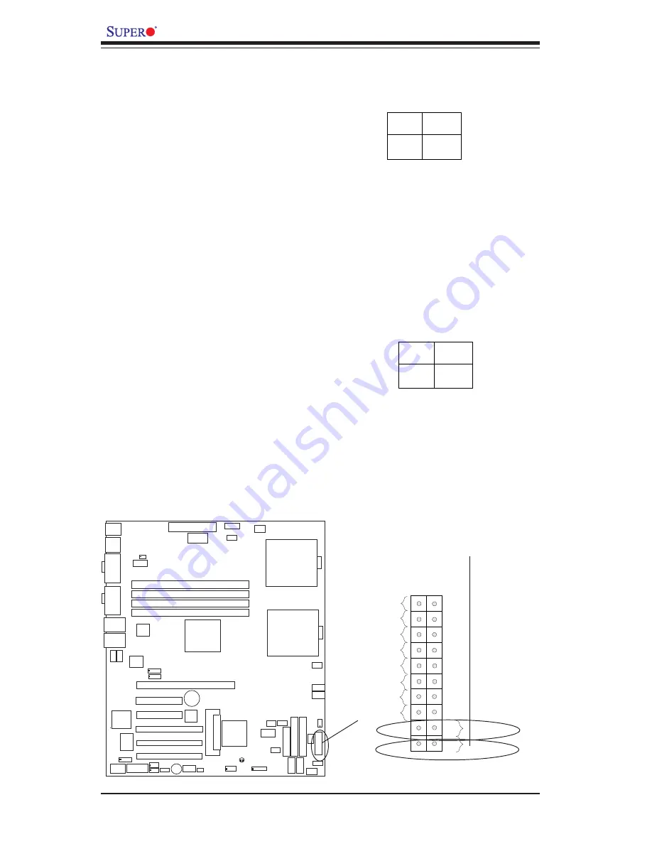
Power Button
The Power Button connection is
located on pins 1 and 2 of JF1.
Momentarily contacting both pins
will power on/off the system. To
turn off the power when set to
suspend mode, press the button
for at least 4 seconds. Refer to
the table on the right for pin defini-
tions.
Pin
Number
1
2
Definition
PW _ON
Ground
Power Button
Connector
Pin Definitions
(JF1)
Reset Button
The Reset Button connection is lo-
cated on pins 3 and 4 of JF1. At-
t a c h i t t o t h e h a r d w a r e r e s e t
s w i t c h o n t h e c o m p u t e r c a s e .
Refer to the table on the right for
pin definitions.
Pin
Number
3
4
Definition
Reset
Ground
Reset Pin
Definitions
(JF1)
P W R
Reset


