Supermicro X11SSL-CF User Manual Download Page 34

34

X11SSL-CF/-nF User Manual
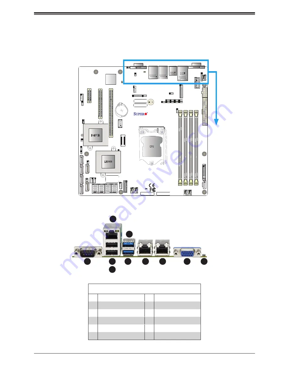
2.5 Rear I/O Ports

See Figure 2-2 below for the locations and descriptions of the various I/O ports on the rear 
of the motherboard.

Figure 2-2. I/O Port Locations and Definitions

Rear I/O Ports

#

Description

#

Description

1.

COM1 Port

6.

USB6 (3.0)

2.

IPMI LAN

7.

LAN1

3

USB1

8

LAN2

4

USB0

9

VGA Port

5.

USB7 (3,.0)

10 UID Switch

1

9

8

7

6

4

3

JPWR2

JPWR1

BMC

Intel PCH

COM2

IPMI_LAN

USB 0/1

COM1

FAN4

JPWR2

USB 6/7 

(3.0)

LAN 1

LAN 2

VGA

JTPM1

JPL1

JPL2

JD1

LED BMC

JIPMB1

JOH1

LE1

JUIDB1

USB 8 (3.0)

LED S1

LED PWR

FAN3

FANA

USB 4/5

USB 9/10 

(3.0)

JSD1

I-SGPIO2

I-SGPIO1

JSD2

JL1

JBT1

JSTBY1

JPS1

X11SSL-CF_(-nF)

REV:1.01

Designed in the USA

MAC CODE

SAS  CODE

SP1

JPG1

JBR1

JPME2

JPB1

JI2C2

SP1

JI2C1

JF1

JPI2C1

FAN1

FAN2

BAR CODE

IPMI CODE

USB 2/3

PCH 
SLOT4 PCI-E 3.0 x1

PCH 
SLOT5 PCI-E 3.0 x4(in x8)

CPU 
SLOT6 PCI-E 3.0 x8(in x16)

I-SA
TA5

I-SA
TA1

I-SA
TA4

I-SA
TA3

I-SA
TA2

I-SA
TA0

JWD1

DIMMB2

DIMMB1

DIMMA2

DIMMA1

JSAS1

JNVME1

LSI 3008

CPU

BT1

MEGERAC

LICENSE

2

5

10

Summary of Contents for X11SSL-CF

Page 1: ...USER MANUAL Revision 1 1 X11SSL CF X11SSL nF...

Page 2: ...a commercial environment This equipment generates uses and can radiate radio frequency energy and if not installed and used in accordance with the manufacturer s instruction manual may cause harmful i...

Page 3: ...oard is intended to be installed and serviced by professional technicians only For processor memory updates please refer to our website at http www supermicro com products SAS 3 0 is available on the...

Page 4: ...ter B V Het Sterrenbeeld 28 5215 ML s Hertogenbosch The Netherlands Tel 31 0 73 6400390 Fax 31 0 73 6416525 Email sales supermicro nl General Information support supermicro nl Technical Support rma su...

Page 5: ...stem Resource Alert 20 1 5 ACPI Features 20 1 6 Power Supply 21 1 7 Serial Port 21 Chapter 2 Installation 2 1 Static Sensitive Devices 22 Precautions 22 Unpacking 22 2 2 Motherboard Installation 23 To...

Page 6: ...em Boot Failure 65 Memory Errors 65 Losing the System s Setup Configuration 66 When the System Becomes Unstable 66 3 2 Technical Support Procedures 68 3 3 Frequently Asked Questions 69 3 4 Battery Rem...

Page 7: ...oftware Installation B 1 Installing Software Programs 109 B 2 SuperDoctor 5 110 Appendix C Standardized Warning Statements Battery Handling 111 Product Disposal 113 Appendix D UEFI BIOS Recovery Appen...

Page 8: ...If anything listed is damaged or missing please contact your retailer 1 1 Checklist Important Links For your system to work properly please follow the links below to download all necessary drivers ut...

Page 9: ...therboard Image Note All graphics shown in this manual were based upon the latest PCB revision available at the time of publication of the manual The motherboard you received may or may not look exact...

Page 10: ...10 X11SSL CF nF User Manual Figure 1 2 X11SSL nF Motherboard Image...

Page 11: ...CF_ nF REV 1 01 Designed in the USA MAC CODE SAS CODE SP1 JPG1 JBR1 JPME2 JPB1 JI2C2 SP1 JI2C1 JF1 JPI2C1 FAN1 FAN2 BAR CODE IPMI CODE USB 2 3 PCH SLOT4 PCI E 3 0 x1 PCH SLOT5 PCI E 3 0 x4 in x8 CPU...

Page 12: ...N3 FANA USB 4 5 USB 9 10 3 0 JSD1 I SGPIO2 I SGPIO1 JSD2 JL1 JBT1 JSTBY1 JPS1 X11SSL CF_ nF REV 1 01 Designed in the USA MAC CODE SAS CODE SP1 JPG1 JBR1 JPME2 JPB1 JI2C2 SP1 JI2C1 JF1 JPI2C1 FAN1 FAN2...

Page 13: ...tive Red SAS Error Connector Description BT1 Onboard Battery COM1 COM2 COM1 COM2 Port Headers Fan1 Fan4 FanA System CPU Fan Headers IPMI_LAN Dedicated IPMI Gigabit RJ45 Port I SATA0 I SATA5 SATA 3 0 C...

Page 14: ...ess 3 0 x8 in x16 Slot PCI E PCH Slot 5 PCI Express 3 0 x4 in x8 Slot PCI E PCH Slot 4 PCI Express 3 0 x1 Slot SP1 Internal Speaker Buzzer USB 0 1 Back Panel USB 2 0 Ports USB 2 3 USB 4 5 Front Access...

Page 15: ...oducts motherboard Chipset Intel PCH C232 Expansion Slots One 1 PCI Express 3 0 x1 slot PCH Slot 4 One 1 PCI Express 3 0 x4 in x8 PCH Slot 5 One 1 PCI Express 3 0 x8 in x16 slot CPU Slot 6 Network Int...

Page 16: ...up from Soft Off CPU fan auto off in sleep mode Main Switch Override Mechanism Wake On LAN WOL Power on mode for AC power recovery Server Platform Service System Health Monitoring Onboard voltage moni...

Page 17: ...hermal design power TDP is subject to chassis and heatsink cooling restrictions For proper thermal management please check the chas sis and heatsink specifications for proper CPU TDP sizing Note 2 For...

Page 18: ...at diff SMBUS TPM HEADER USB 3 0 USB BIOS SPI AST2400 BMC PCIe 7 RMII NCSI COM1 Connector COM2 Header VGA CONN BMC Boot Flash DDR3 3 PHASE for Vcore 80W IMVP 8 DMI3 x4 DMI3 Skt H4 LGA1151 I210 LAN 1 2...

Page 19: ...ng PCI E 3 0 SATA 3 0 with transfer rates of up to 6 Gb s xHCI USB with SuperSpeed 3 0 System Management Bus SMBus Specification Version 2 0 Integrated Sensor Hub ISH Intel Trusted Execution Technolog...

Page 20: ...r the temperature of the CPU or the system exceeds a user defined threshold system CPU cooling fans will be turned on to prevent the CPU or the system from overheating Note To avoid possible system ov...

Page 21: ...hat contains a 24 pin and an 8 pin power connector Be sure to connect the power supplies to the 24 pin power connector JPWR1 and the 8 pin power con nector JPWR2 on the motherboard Failure in doing so...

Page 22: ...h its components peripheral chips memory modules or gold contacts When handling chips or modules avoid touching their pins Put the motherboard and peripherals back into their antistatic bags when not...

Page 23: ...lation All motherboards have standard mounting holes to fit different types of chassis Make sure that the locations of all the mounting holes for both the motherboard and the chassis match Although a...

Page 24: ...l standoffs in the chassis as needed 5 Install the motherboard into the chassis carefully to avoid damaging other motherboard components 6 Using the Phillips screwdriver insert a Phillips head 6 screw...

Page 25: ...uy a CPU separately make sure that you use an Intel certified multi directional heatsink only Make sure to install the motherboard into the chassis before you install the CPU heatsink When receiving a...

Page 26: ...e your thumb and your index finger to hold the CPU at the North center edge and the South center edge of the CPU 4 Align the CPU key that is the semi circle cutouts against the socket keys Once it is...

Page 27: ...your CPU Instead open the load plate again and double check that the CPU is aligned properly CPU properly installed Load lever locked into place 5 Do not rub the CPU against the surface or against any...

Page 28: ...routed through the bottom of the heatsink 4 Remove the thin layer of the protective film from the heatsink Important CPU overheating may oc cur if the protective film is not removed from the heatsink...

Page 29: ...until you hear a click Also make sure to orient each fastener so that the narrow end of the groove is pointing outward 8 Repeat step 7 to insert all four heatsink fasteners into the mounting holes 9...

Page 30: ...or other components Active Heatsink Removal 1 Unplug the power cord from the power supply 2 Disconnect the heatsink fan wires from the CPU fan header 3 Use your finger tips to gently press on the fas...

Page 31: ...performance follow the table below when populating memory Processors and their Corresponding Memory Modules CPU Corresponding DIMM Modules CPU DIMMA1 DIMMA2 DIMMB1 DIMMB2 Memory Module Population for...

Page 32: ...ot DIMMA2 Blue Slot Towards the edge of the motherboard Towards the CPU DIMMA1 DIMMB1 JPWR2 JPWR1 BMC Intel PCH COM2 IPMI_LAN USB 0 1 COM1 FAN4 JPWR2 USB 6 7 3 0 LAN 1 LAN 2 VGA JTPM1 JPL1 JPL2 JD1 LE...

Page 33: ...ber of DIMMs into the memory slots starting with DIMMB2 Channel B Slot 2 blue slot For best performance please use the memory modules of the same type and speed in the same bank 2 Push the release tab...

Page 34: ...2 IPMI_LAN USB 0 1 COM1 FAN4 JPWR2 USB 6 7 3 0 LAN 1 LAN 2 VGA JTPM1 JPL1 JPL2 JD1 LED BMC JIPMB1 JOH1 LE1 JUIDB1 USB 8 3 0 LED S1 LED PWR FAN3 FANA USB 4 5 USB 9 10 3 0 JSD1 I SGPIO2 I SGPIO1 JSD2 JL...

Page 35: ...DE SAS CODE SP1 JPG1 JBR1 JPME2 JPB1 JI2C2 SP1 JI2C1 JF1 JPI2C1 FAN1 FAN2 BAR CODE IPMI CODE USB 2 3 PCH SLOT4 PCI E 3 0 x1 PCH SLOT5 PCI E 3 0 x4 in x8 CPU SLOT6 PCI E 3 0 x8 in x16 I SATA5 I SATA1 I...

Page 36: ...LSI 3008 CPU BT1 MEGERAC LICENSE 1 2 1 LAN1 2 LAN2 3 IPMI LAN 3 LAN Ports Two Gigabit Ethernet ports LAN1 and LAN2 are located on the I O back panel on the motherboard In addition a dedicated IPMI LAN...

Page 37: ...he tables below for pin definitions Back Panel USB 0 1 2 0 Pin Definitions Pin Definition Pin Definition 1 5V 5 5V 2 USB_N 6 USB_N 3 USB_P 7 USB_P 4 Ground 8 Ground Front Panel USB 2 3 4 5 2 0 Pin Def...

Page 38: ...round 8 SSTX 9 SSTX 4 5 6 JPWR2 JPWR1 BMC Intel PCH COM2 IPMI_LAN USB 0 1 COM1 FAN4 JPWR2 USB 6 7 3 0 LAN 1 LAN 2 VGA JTPM1 JPL1 JPL2 JD1 LED BMC JIPMB1 JOH1 LE1 JUIDB1 USB 8 3 0 LED S1 LED PWR FAN3 F...

Page 39: ...SL CF_ nF REV 1 01 Designed in the USA MAC CODE SAS CODE SP1 JPG1 JBR1 JPME2 JPB1 JI2C2 SP1 JI2C1 JF1 JPI2C1 FAN1 FAN2 BAR CODE IPMI CODE USB 2 3 PCH SLOT4 PCI E 3 0 x1 PCH SLOT5 PCI E 3 0 x4 in x8 CP...

Page 40: ...ystem This button can also be configured to function as a suspend button with a setting in the BIOS see Chapter 4 To turn off the power when the system is in suspend mode press the button for 4 second...

Page 41: ...arnings of overheat or fan failure Refer to the tables below for pin definitions OH Fan Fail Indicator Status State Definition Off Normal On Overheat Flashing Fan Fail OH Fan Fail LED Pin Definitions...

Page 42: ...D UID Switch The HDD LED UID Switch connection is located on pins 13 and 14 of JF1 Attach a cable to pin 14 to show hard drive activity status Attach a cable to pin 13 to use UID switch Refer to the t...

Page 43: ...n definitions Power Fail LED Pin Definitions JF1 Pin Definition 19 3 3V 20 PWR Supply Fail Power Button Blue OH Fan Fail 1 NIC1 Link LED Reset Button 2 Power Fail LED HDD LED FP PWRLED Reset PWR 3 3 V...

Page 44: ...V 11 12V 24 COM 12 3 3V Required Connection JPWR2 JPWR1 BMC Intel PCH COM2 IPMI_LAN USB 0 1 COM1 FAN4 JPWR2 USB 6 7 3 0 LAN 1 LAN 2 VGA JTPM1 JPL1 JPL2 JD1 LED BMC JIPMB1 JOH1 LE1 JUIDB1 USB 8 3 0 LED...

Page 45: ...TPM1 JPL1 JPL2 JD1 LED BMC JIPMB1 JOH1 LE1 JUIDB1 USB 8 3 0 LED S1 LED PWR FAN3 FANA USB 4 5 USB 9 10 3 0 JSD1 I SGPIO2 I SGPIO1 JSD2 JL1 JBT1 JSTBY1 JPS1 X11SSL CF_ nF REV 1 01 Designed in the USA MA...

Page 46: ...C JIPMB1 JOH1 LE1 JUIDB1 USB 8 3 0 LED S1 LED PWR FAN3 FANA USB 4 5 USB 9 10 3 0 JSD1 I SGPIO2 I SGPIO1 JSD2 JL1 JBT1 JSTBY1 JPS1 X11SSL CF_ nF REV 1 01 Designed in the USA MAC CODE SAS CODE SP1 JPG1...

Page 47: ...1 Internal Buzzer 2 Speaker Header Internal Speaker Buzzer The Internal Speaker SP1 can be used to provide audible notifications using various beep codes Refer to the table below for pin definitions R...

Page 48: ...I SATA3 I SATA2 I SATA0 JWD1 DIMMB2 DIMMB1 DIMMA2 DIMMA1 JSAS1 JNVME1 LSI 3008 CPU BT1 MEGERAC LICENSE 1 1 DOM PWR1 2 DOM PWR2 3 Chassis Intrusion Disk On Module Power Connector Two power connectors f...

Page 49: ...JWD1 DIMMB2 DIMMB1 DIMMA2 DIMMA1 JSAS1 JNVME1 LSI 3008 CPU BT1 MEGERAC LICENSE 1 2 1 I SGPIO1 2 I SGPIO2 3 PWR SMB SGPIO Headers Two I SGPIO Serial Link General Purpose Input Output headers are locate...

Page 50: ...E 3 0 x4 in x8 CPU SLOT6 PCI E 3 0 x8 in x16 I SATA5 I SATA1 I SATA4 I SATA3 I SATA2 I SATA0 JWD1 DIMMB2 DIMMB1 DIMMA2 DIMMA1 JSAS1 JNVME1 LSI 3008 CPU BT1 MEGERAC LICENSE 1 1 JTPM1 Trusted Platform...

Page 51: ...DIMMB1 DIMMA2 DIMMA1 JSAS1 JNVME1 LSI 3008 CPU BT1 MEGERAC LICENSE 1 2 1 IPMB 2 Overheat LED 4 pin BMC External I2 C Header A System Management Bus header for IPMI 2 0 is located at JIPMB1 Connect th...

Page 52: ...er s guide posted on our website at http www supermicro com SATA 3 0 Port Pin Definitions Pin Signal 1 Ground 2 SATA_TXP 3 SATA_TXN 4 Ground 5 SATA_RXN 6 SATA_RXP 7 Ground X11SSL CF nF SATA 3 0 Connec...

Page 53: ...rformance and significantly reduces PCI E latency by simplifying driver software requirements JPWR2 JPWR1 BMC Intel PCH COM2 IPMI_LAN USB 0 1 COM1 FAN4 JPWR2 USB 6 7 3 0 LAN 1 LAN 2 VGA JTPM1 JPL1 JPL...

Page 54: ...entifier Switch UID LED Indicator A rear Unit Identifier UID switch and a rear UID LED LE1 are located next to the VGA port on the motherboard The front UID switch and the front UID LED are both locat...

Page 55: ...tween two pins to change the function of the connector Pin 1 is identified with a square solder pad on the printed circuit board See the diagram below for an example of jumping pins 1 and 2 Refer to t...

Page 56: ...SATA3 I SATA2 I SATA0 JWD1 DIMMB2 DIMMB1 DIMMA2 DIMMA1 JSAS1 JNVME1 LSI 3008 CPU BT1 MEGERAC LICENSE 1 2 LAN Port Enable Disable Change the setting of jumper JPL1 JPL2 to enable or disable the LAN1 LA...

Page 57: ...atch Dog 2 JI2 C1 3 JI2 C2 2 Watch Dog Watch Dog JWD1 is a system monitor that can reboot the system when a software application hangs Close pins 1 2 to reset the system if an application hangs Close...

Page 58: ...SATA1 I SATA4 I SATA3 I SATA2 I SATA0 JWD1 DIMMB2 DIMMB1 DIMMA2 DIMMA1 JSAS1 JNVME1 LSI 3008 CPU BT1 MEGERAC LICENSE 1 1 VGA Enable 2 BIOS Recovery Enable 2 VGA Enable Disable Jumper JPG1 allows the...

Page 59: ...MMA1 JSAS1 JNVME1 LSI 3008 CPU BT1 MEGERAC LICENSE 1 1 Manufacterer Mode Select 2 SAS Status 2 Manufacturer Mode Select Close pin 2 and pin 3 of jumper JPME2 to bypass SPI flash security and force the...

Page 60: ...C1 JF1 JPI2C1 FAN1 FAN2 BAR CODE IPMI CODE USB 2 3 PCH SLOT4 PCI E 3 0 x1 PCH SLOT5 PCI E 3 0 x4 in x8 CPU SLOT6 PCI E 3 0 x8 in x16 I SATA5 I SATA1 I SATA4 I SATA3 I SATA2 I SATA0 JWD1 DIMMB2 DIMMB1...

Page 61: ...ports LAN 1 and LAN 2 are located on the I O back panel of the motherboard Each Ethernet LAN port has two LEDs The green LED indicates activity while the other Link LED may be green amber or off to i...

Page 62: ...SATA0 JWD1 DIMMB2 DIMMB1 DIMMA2 DIMMA1 JSAS1 JNVME1 LSI 3008 CPU BT1 MEGERAC LICENSE 1 1 Onboard Power LED 2 BMC Heartbeat LED 2 Onboard Power LED The Onboard Power LED is located at LEDPWR on the mot...

Page 63: ...4 5 USB 9 10 3 0 JSD1 I SGPIO2 I SGPIO1 JSD2 JL1 JBT1 JSTBY1 JPS1 X11SSL CF_ nF REV 1 01 Designed in the USA MAC CODE SAS CODE SP1 JPG1 JBR1 JPME2 JPB1 JI2C2 SP1 JI2C1 JF1 JPI2C1 FAN1 FAN2 BAR CODE IP...

Page 64: ...ose for the keyboard and mouse 3 Remove all add on cards 4 Install the CPU first making sure it is fully seated and connect the front panel connectors to the motherboard No Power 1 Make sure that ther...

Page 65: ...module installed If the system boots check for bad DIMM modules or slots by following the Memory Errors Troubleshooting procedure in this Chapter Memory Errors When a no memory beep code is issued by...

Page 66: ...http www supermicro com for memory and CPU support and updates 3 HDD support Make sure that all hard disk drives HDDs work properly Replace the bad HDDs with good ones 4 System cooling Check the syste...

Page 67: ...necessary remove a component in question from the chassis and test it in isolation to make sure that it works properly Replace a bad component with a good one 5 Check and change one component at a ti...

Page 68: ...pter or see the FAQs on our website http www supermicro com before contacting Technical Support 2 BIOS upgrades can be downloaded from our website http www supermicro com 3 If you still cannot resolve...

Page 69: ...BIOS on our website Select your motherboard model and download the BIOS file to your computer Also check the current BIOS revision to make sure that it is newer than your BIOS before downloading You c...

Page 70: ...the battery in any way a damaged battery may release hazardous materials into the environment Do not discard a used battery in the garbage or a public landfill Please comply with the regulations set...

Page 71: ...displayed on the outside of the shipping carton and the shipping package is mailed prepaid or hand carried Shipping and handling charges will be applied for all orders that must be mailed when service...

Page 72: ...IOS screen has two main frames The left frame displays all the options that can be configured Grayed out options cannot be configured The right frame displays the key legend Above the key legend is an...

Page 73: ...lease refer to the UEFI BIOS Recovery User Guide posted at http www supermicro com support manuals System Date System Time Use this option to change the system date and time Highlight System Date or S...

Page 74: ...CF nF User Manual 74 Memory Information Total Memory This feature displays the total size of memory available in the system Memory Speed This feature displays the speed of memory modules used in the...

Page 75: ...OST messages The options are Enabled and Disabled AddOn ROM Display Mode Use this feature to set the display mode for the Option ROM Select Keep Current to display the current AddOn ROM setting Select...

Page 76: ...ow the system to reset or generate NMI signals based on the Watch Dog jumper setting when the system is inactive more than 5 minutes The options are Disabled and Enabled Power Button Function This fea...

Page 77: ...che L3 Cache L4 Cache Hyper threading Available when supported by the CPU Select Enabled to support Intel Hyper threading Technology to enhance CPU performance The options are Enabled and Disabled Act...

Page 78: ...both cache lines for 128 bytes as comprised The options are Disabled and Enabled CPU AES Select Enabled to enable Intel CPU Advanced Encryption Standard AES Instructions for CPU to enhance data integr...

Page 79: ...Window in seconds The value may vary from 0 to 128 If the value is set to 0 a default value will be used 28 sec for Mobile and 1 sec for Desktop The options are 0 1 2 3 4 5 6 7 8 10 12 14 16 20 24 28...

Page 80: ...the enhanced C State of the CPU The options are Disabled and Enabled C State Auto Demotion Use this feature to prevent unnecessary excursions into the C states to improve latency The options are Disa...

Page 81: ...nt Bridge Name SA PCIe Code Version VT d VT d Select Enabled to enable Intel Virtualization Technology support for Direct I O VT d by reporting the I O device assignments to VMM through the DMAR ACPI...

Page 82: ...d CPU DMI Link ASPM Control Use this feature to set the ASPM Active State Power Management state on the SA System Agent side of the DMI Link The options are Disabled and L1 DMI Extended Sync Control U...

Page 83: ...to manage power consumption of serial link devices installed on PCI Exp slots during a prolonged off peak time If this item is set to Enabled PCI E ASMP will be programmed after OPROM If this item is...

Page 84: ...enable or disable fast path through the memory reference codes The options are Enabled and Disabled REFRESH_2X_MODE Use this feature to select the refresh mode The options are Disabled 1 Enabled for W...

Page 85: ...The options are Auto Gen1 Gen2 and Gen3 Port 8 Detect Non Compliance Device If this feature is set to Enabled the AMI BIOS will automatically detect a PCI E device installed on the port specified that...

Page 86: ...nd Enabled SATA Configuration When this submenu is selected the AMI BIOS automatically detects the presence of the SATA devices that are supported by the Intel PCH chip and displays the following item...

Page 87: ...r SATA Frozen Use this feature to enable the HDD Security Frozen Mode The options are Disabled and Enabled Serial ATA Port 0 Port 5 This feature displays the information detected on the installed SATA...

Page 88: ...system boot The options are Disabled Legacy and EFI PCH SLOT5 PCI E 3 0 X4 IN X8 OPROM Use this feature to select which firmware type to be loaded for the add on card in this slot for system boot The...

Page 89: ...e default setting is 0 Media detect count Use this option to specify the number of times media will be checked Press or on your keyboard to change the value The default setting is 1 Super IO Configura...

Page 90: ...feature specifies the base I O port address and the Interrupt Request address of a serial port specified by the user Select Auto to allow the BIOS to automatically assign the base I O and IRQ address...

Page 91: ...minal Type This feature allows the user to select the target terminal emulation type for Console Redirection Select VT100 to use the ASCII Character set Select VT100 to add color and function key supp...

Page 92: ...on to prevent data loss caused by buffer overflow Send a Stop signal to stop sending data when the receiving buffer is full Send a Start signal to start sending data when the receiving buffer is empty...

Page 93: ...upport Select ANSI to use the Extended ASCII Character Set Select VT UTF8 to use UTF8 encoding to map Unicode characters into one or more bytes The options are VT100 VT100 VT UTF8 and ANSI COM2 Bits P...

Page 94: ...al resolution support The options are Disabled and Enabled COM2 Legacy OS Redirection Resolution Use this feature to select the number of rows and columns used in Console Redirection for legacy OS sup...

Page 95: ...for a serial port used in Console Redirection Make sure that the same speed is used in the host computer and the client computer A lower transmission speed may be required for long and busy lines The...

Page 96: ...s Hardware Error Architecture WHEA support for the Windows 2008 or a later version operating system The options are Disabled and Enabled Trusted Computing Available when a TPM device is installed and...

Page 97: ...s feature allows the user to enter the unique name of the iSCSI Initiator in the IQN format Once the name of the iSCSI Initiator is entered into the system configure the proper settings for the follow...

Page 98: ...Erase Event Log Select Yes to erase all error events in the SMBIOS System Management BIOS log before an event logging is initialized at bootup The options are No Yes Next reset and Yes every reset Whe...

Page 99: ...This feature is used to determine how long in minutes the multiple event counter should wait before generating a new event log Enter a number between 0 to 99 The default setting is 60 Note Please rebo...

Page 100: ...m event logs upon each system reboot Select No to keep all system event logs after each system reboot The options are No Yes On next reset and Yes On every reset When SEL is Full This feature allows t...

Page 101: ...lected AMI BIOS will search for a DHCP Dynamic Host Configuration Protocol server attached to the network and request the next available IP address for this computer The options are DHCP and Static St...

Page 102: ...lways Administrator Password Press Enter to create a new administrator password or change an existing administrator password User Password Press Enter to create a new user password or to change an exi...

Page 103: ...install factory default secure boot keys The options are Enabled and Disabled Enroll All Factory Default Keys This feature allows the user to store security related boot data in a file of the same na...

Page 104: ...able devices from which the system will boot Press Enter on each entry from top to bottom to select devices When the feature above Boot Mode Select is set to Dual default the following items will be d...

Page 105: ...d to the boot priority list Delete Boot Option Use this feature to select a boot device to delete from the boot priority list Delete Boot Option Use this feature to select the target boot device to de...

Page 106: ...ption to leave the BIOS setup utility and reboot the computer so that the new system configuration parameters can take effect Select Save Changes and Exit from the Exit menu and press Enter Save Chang...

Page 107: ...ings for future use Restore User Defaults Select this option and press Enter to retrieve user defined settings that were saved previously Boot Override Listed on this section are other boot options fo...

Page 108: ...rors are usually communicated through a series of audible beeps The numbers on the fatal error list correspond to the number of beeps for the corresponding error BIOS Beep POST Codes Beep Code Error M...

Page 109: ...nd utilities it contains You may also use a utility to extract the ISO file if preferred After creating a DVD with the ISO files insert the disk into the DVD drive on your system and the display shown...

Page 110: ...re system voltages system power consumption fan speed and provides alerts via email or Simple Network Management Protocol SNMP SuperDoctor 5 comes in local and remote management versions and can be us...

Page 111: ...e installing or configuring components These warnings may also be found on our website at http www supermicro com about policies safety_information cfm Battery Handling Warnung Bei Einsetzen einer fal...

Page 112: ...aar indien de batterij verkeerd vervangen wordt Vervang de batterij slechts met hetzelfde of een equivalent type die door de fabrikant aanbevolen wordt Gebruikte batterijen dienen overeenkomstig fabri...

Page 113: ...tos nacionales Attention La mise au rebut ou le recyclage de ce produit sont g n ralement soumis des lois et ou directives de respect de l environnement Renseignez vous aupr s de l organisme comp tent...

Page 114: ...he recovery block contains critical BIOS codes including memory detection and recovery codes for the user to flash a healthy BIOS image if the original main BIOS image is corrupted When the system pow...

Page 115: ...u cannot locate the Super ROM file in your drive disk visit our website at www supermicro com to download the BIOS package Extract the BIOS binary image into a USB flash device and rename it Super ROM...

Page 116: ...u want to start the BIOS recovery If you decide to proceed with BIOS recovery follow the procedures below 4 When the screen as shown above displays use the arrow keys to select the item Proceed with f...

Page 117: ...Do not interrupt this process until the BIOS flashing is complete 8 After seeing the message indicating the BIOS update has completed unplug the AC power cable from the power supply clear CMOS then p...

Page 118: ...to a software tool issue see image below or an unexpected power outage during BIOS updates BIOS Boot Block Corruption Occurrence When a BIOS boot block is corrupted due to an unexpected power outage...

Page 119: ...per JBR1 1 Power down the system 2 Close pins 2 3 on jumper JBR1 and power on the system 3 Follow the BIOS recovery SOP listed in the previous chapter Appendix D 4 After completing the steps above pow...

Reviews: