


OXY5740A
User’s Manual
Revision Date: November 11 2019
11
2.2 Jumper Settings
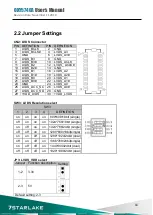
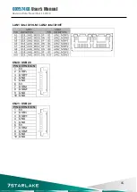
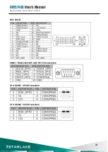
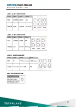
CN2: LVDS Connector
PIN DEFINITION
PIN DEFINITION
1
LVDS_BCLK
2
GND
3
LVDS_BCLK#
4
LVDS_A3
5
GND
6
LVDS_A3#
7
LVDS_B3
8
GND
9
LVDS_B3#
10 LVDS_ACLK
11
LVDS_B2
12 LVDS_ ACLK #
13 LVDS_B2#
14 GND
15 LVDS_B1
16 LVDS_A2
17 LVDS_B1#
18 LVDS_A2#
19 LVDS_B0
20 LVDS_A1
21 LVDS_B0#
22 LVDS_A1#
23 GND
24 LVDS_A0
25 LVDS_DCC_SC
26 LVDS_A0#
27 LVDS_DCC_SD
28 GND
29 +VDD_LVDS
30 +VDD_LVDS
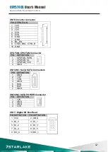
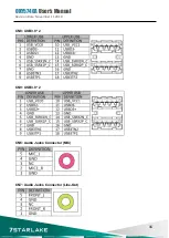
SW3: LVDS Resolution select
SW3
1
2
3
4
DEFINITION
on
on
on
on
800*600/18bit (single)
off
on
on
on 1024*768/18bit (single)
on
off
on
on 1024*768/24bit (single)
off
off
on
on
1280*800/18bit(single)
on
on
off
on
1280*1024/24bit (dual)
off
on
off
on
1366*768/24bit(single)
on
off
off
on
1440*900/24bit (dual)
off
off
off
on
1920*1080/24bit (dual)
JP3: LVDS_VDD select
Jumper Function description Setting
1-2
3.3V
2-3
5V
Default setting: 2-3
Summary of Contents for OXY5740A
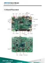
Page 9: ...OXY5740A User s Manual Revision Date November 11 2019 8 1 3 Board Placement ...
Page 15: ...OXY5740A User s Manual Revision Date November 11 2019 14 MCARD2 Mini PCIE Card Slot ...
Page 22: ...OXY5740A User s Manual Revision Date November 11 2019 21 CON A1 CONNECTOR A TOP ...
Page 23: ...OXY5740A User s Manual Revision Date November 11 2019 22 FPE1 StackPC FPE Top Connector ...
Page 34: ...OXY5740A User s Manual Revision Date November 11 2019 33 ...
Page 35: ...OXY5740A User s Manual Revision Date November 11 2019 34 4 4 6 Hardware Monitor ...
Page 36: ...OXY5740A User s Manual Revision Date November 11 2019 35 4 4 7 CSM Configuration 4 5 Chipset ...


