
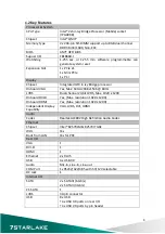

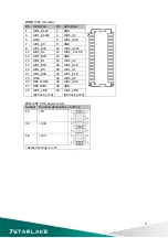
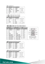

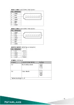


LVDS:
LVDS
connector
Pin
Definition
Pin
Definition
1
LVDS_BCLK
2
GND
3
LVDS_BCLK#
4
LVDS_A3
5
GND
6
LVDS_A3#
7
LVDS_B3
8
GND
9
LVDS_B3#
10
LVDS_ACLK
11
LVDS_B2
12
LVDS_
ACLK
#
13
LVDS_B2#
14
GND
15
LVDS_B1
16
LVDS_A2
17
LVDS_B1#
18
LVDS_A2#
19
LVDS_B0
20
LVDS_A1
21
LVDS_B0#
22
LVDS_A1#
23
GND
24
LVDS_A0
25
DDC
CLOCK
26
LVDS_A0#
27
DDC
DATA
28
GND
29
LVDS_VDD
(Define
by
JP4)
30
LVDS_VDD
(Define
by
JP4)
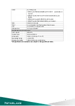
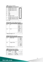
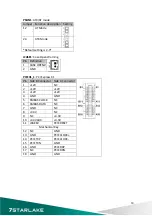
JP4:
LVDS_VDD
power
select
Jumper
Function
description
Setting
1
‐
2
+5V
3
‐
4
+3.3V
5
‐
6
+12V
*Default
setting
is
3
‐
4*
11
Summary of Contents for INS8335A
Page 1: ...INS8335A Mini ITX Industrial Motherboard User s Manual ...
Page 5: ...3 8 Save and exit 48 4 ...
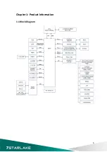
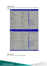
Page 6: ...Chapter 1 Product Information 1 1 Block Diagram 5 ...
Page 9: ...1 3 Board Placement 8 ...
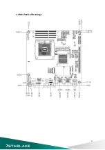
Page 10: ...1 4 Mechanical Drawings 9 ...
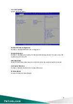
Page 27: ...3 4 2 CPU Configuration This section is used to configure the CPU 26 ...
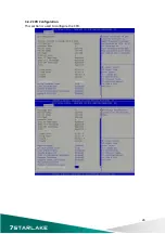
Page 31: ...3 4 5 Intel Rapid Start Technology 30 ...