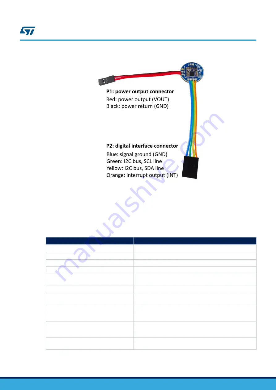
ST STEVAL-ISB68WA User Manual Download Page 4

Figure 4. 

Receiver module wiring

Additional control signals and programmable general-purpose I/O pins are available at the STWLC68JRH, but
they are not used in the module to keep the reference solution as simple as possible. The STWLC68JRH chip can
handle up to 400 kHz speed over the I2C bus. 

Table 2

 summarizes the default STWLC68JRH settings that are

retrieved from OTP memory at power-up. Values eventually changed via I2C registers are lost if the receiver
module is removed from the transmitter, unless VOUT or VRECT rails are externally kept above 4V (e.g. as per

Figure 7

b).

Table 2. 

Receiver module default settings

Parameter

Default setting

Output voltage

5.0 V

Minimum VRECT

4 V (output is disconnected if VRECT voltage is lower than this value)

Dummy load

40 mA (minimum load current to ensure ASK communication stability)

Nominal chip idle current consumption

17 mA (application dependent)

Output current threshold for deeper ASK

modulation

100 mA (if the output current is higher than this value, auxiliary

modulation pins CLAMP1 and CLAMP2 are activated)

GPIO0 pin function

Open drain, low when output is enabled (D3 LED)

INT pin function

Open-drain, low in case of over-temperature, over-current or over-

voltage condition.

Over-Temperature protection

Lower 80°C threshold leading to output disconnection and EPT

generation to terminate power transfer. Upper 125°C threshold leading to

AC1 and AC2 pins short-to-ground.

Over-Voltage protection (VRECT rail)

Lower 12 V threshold leading to temporary IEXT activation (VRECT

clamping). Upper 25 V threshold leading to AC1 and AC2 pins short-to-

ground.

Over-Current protection

1.5 A threshold leading to output disconnection and EPT generation to

terminate the power transfer.

UM2693

Wireless power receiver module

UM2693

 - 

Rev 1

page 4/18

Summary of Contents for STEVAL-ISB68WA

Page 1: ...2 5 W and it works out of the box when placed on a suitable wireless power transmitter An on board LED indicates when the communication with the transmitter succeeds and the power transfer is in prog...

Page 2: ...l VOUT pins is filtered by C18 through C20 capacitors and made available at J5 terminal Few additional components are needed to complete the wireless receiver bootstrap capacitors for the rectifier C8...

Page 3: ...nnectors Figure 4 Table 1 Receiver module terminals Terminal Signal Wiring color J1 AC input RX coil J2 AC input RX coil J3 VRECT rectifier output J4 Power return ground Black P1 J5 VOUT power output...

Page 4: ...to ensure ASK communication stability Nominal chip idle current consumption 17 mA application dependent Output current threshold for deeper ASK modulation 100 mA if the output current is higher than t...

Page 5: ...8101219 Wurth C1 C2 C3 47nF 10 MLCC X7R 50V 0402 GRM155R71H473KE14D Murata C4 100nF 10 GCM155R71H104KE02D C5 1 8nF 5 GRM155R71H182JA01D C7 C8 C10 C11 47nF 10 GRM155R71H473KE14D C12 4n7 10 GCM155R71H47...

Page 6: ...3 I O2 4 VBUS 5 I O1 6 U3 USBCL6 2 GP0 1 GP1 2 RST 3 URx 4 UTx 5 GP2 6 GP3 7 SDA 8 SCL 9 VUSB 10 D 11 D 12 VSS 13 NC 14 NC 15 VDD 16 U1 MCP2221 RST VBUS 1 D 2 D 3 ID 4 GND 5 Shield Shell P1 MicroUSB...

Page 7: ...way of powering the receiver module is also required during OTP memory flashing Figure 7 Connection between receiver module and dongle Table 5 USB to I2C bridging dongle bill of material Component Val...

Page 8: ...603 0603L025 Littelfuse U1 USB to I2C converter QFN16 MCP2221A I ML Microchip U2 Linear regulator 3 3V 100 mA SOT23 5L LD2981CM33TR STMicroelectronics U3 ESD suppressor SOT23 USBCL6 2SC6 STMicroelectr...

Page 9: ...er transmitter evaluation kit contains the reference transmitter for the test setup The complete test setup is shown in Figure 8 Figure 8 STEVAL ISB68WA evaluation setup The receiver is connected to t...

Page 10: ...the LED on the receiver lights up its control GUI can be launched Connectivity with the STWLC68JRH is automatically verified and the chip info IDs content is shown in the registers page Figure 10 UM26...

Page 11: ...a real time plotting of key parameters can be selected in Figure 11 the VRECT and VOUT voltages the temperature of the rectifier TRECT and its output current ISNS are shown Figure 11 Graphical User In...

Page 12: ...6 V via GUI Note that increasing the output voltage may impact on the external components e g proximity to maximum voltage rating of VRECT and VOUT capacitors or to clamping voltage of protection TVS...

Page 13: ...Figure 13 Transmitter input to receiver output overall efficiency UM2693 STEVAL ISB68WA test setup UM2693 Rev 1 page 13 18...

Page 14: ...Revision history Table 6 Document revision history Date Version Changes 19 Feb 2020 1 Initial release UM2693 UM2693 Rev 1 page 14 18...

Page 15: ...s 1 Wireless power receiver module 2 2 USB to I2C bridging dongle 6 3 STEVAL ISB68WA test setup 9 Revision history 14 Contents 15 List of tables 16 List of figures 17 UM2693 Contents UM2693 Rev 1 page...

Page 16: ...eiver module default settings 4 Table 3 Receiver module bill of material 5 Table 4 USB to I2C bridging dongle P2 connector 6 Table 5 USB to I2C bridging dongle bill of material 7 Table 6 Document revi...

Page 17: ...ure 7 Connection between receiver module and dongle 7 Figure 8 STEVAL ISB68WA evaluation setup 9 Figure 9 Configuration of the transmitter 10 Figure 10 Graphical User Interface registers page showing...

Page 18: ...ts and ST assumes no liability for application assistance or the design of Purchasers products No license express or implied to any intellectual property right is granted by ST herein Resale of ST pro...

Reviews: