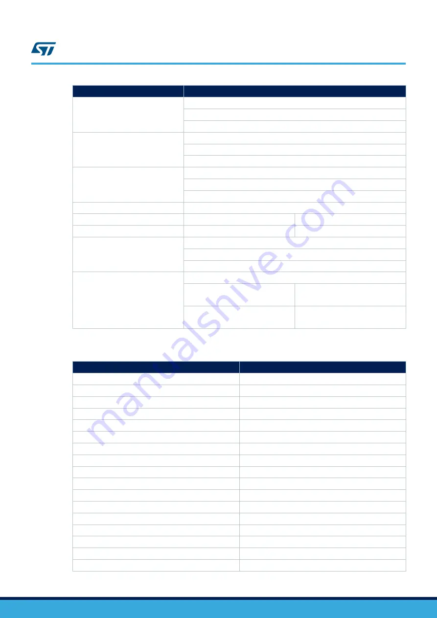
ST STEVAL-IPMM10B User Manual Download Page 21

Jumper

Description

SW1

To choose current U to send to control board:

Jumper on 1-2: from amplification

Jumper on 2-3: directly from motor output

SW2

To choose current V to send to control board

Jumper on 1-2: from amplification

Jumper on 2-3: directly from motor output

SW4

To choose current W to send to control board:

Jumper on 1-2: from amplification

Jumper on 2-3: directly from motor output

SW13

To modify phase A hall sensor network

SW14

To modify phase B hall sensor network

SW15

To modify phase C hall sensor network

SW9, SW16

To choose input power for Hall/Encoder

Jumper on 1-2: 5 V

Jumper on 2-3: 3.3 V

SW5, SW6SW7, SW8

To choose one-shunt or three-shunt configuration. (Through solder bridge)

SW5, SW6 closed

SW7, SW8 open

one shunt

SW5, SW6 open

SW7, SW8 closed

three shunt

Table 8. 

Test pins

Test pin

Description

TP1

NTC (T2 pin)

TP2

VBOOTw

TP3

VBOOTv

TP4

VBOOTu

TP5

HinU (high side U control signal input)

TP6

HinV (high side V control signal input)

TP7

HinW (high side W control signal input)

TP8

VCCH

TP9

phase A (U pin)

TP10

phase B (V pin)

TP11

Ground

TP12

LinU (high side U control signal input)

TP13

phase C (W pin)

TP14

LinV (high side V control signal input)

TP15

LinW (high side W control signal input)

TP16

Negative DC input for U phase

TP17

CIN

UM2702

Connectors, jumpers and test pins

UM2702

 - 

Rev 1

page 21/34

Summary of Contents for STEVAL-IPMM10B

Page 1: ...hardware short circuit protection fault event and temperature monitoring In order to increase the flexibility it is designed to work in single or three shunt configuration and with double current sens...

Page 2: ...network Two options for current sensing dedicated op amps or through MCU Overcurrent hardware protection IPM temperature monitoring and protection Hall sensor or encoder input MOSFET intelligent powe...

Page 3: ...toring single three shunt resistors and filters for input signals It also includes bypass capacitors for VCC and bootstrap capacitors The capacitors are located very close to the drive IC to avoid mal...

Page 4: ...N M X L 3 3V Bus 3 3V 1 65V Bus_voltage RC6 0 RC2 0 RC12 0 D1 BAT48JFILM RC1 0 C4 47u 35V RC13 0 J1 INPUT dc 1 2 RC10 0 RC7 0 R2 470K R3 120R R1 470K R6 1k0 U1D TSV994 12 13 14 4 11 RC3 0 RC8 0 RC4 0...

Page 5: ...ef M_phase_A M_phase_B Bus_voltage M_phase_C TSO NTC Current_B_amp E2 Current_C_amp E3 Current_A_amp E1 J3 Motor Output 1 2 3 SW2 1 2 3 SW4 1 2 3 SW3 1 2 3 J2 Control Connector 1 2 3 4 5 6 7 8 9 10 11...

Page 6: ...CCH 8 NV 19 NU 20 W 21 V 22 U 23 P 24 T2 25 T1 26 TSO 17 TP2 R10 12k R27 0 08 R11 3k3 R8 1k0 R22 3k3 R16 3k3 SW5 C8 100n TP6 C14 10p TP18 R7 3k9 TP13 R23 1k0 TP8 R17 3k9 R13 3k9 C20 330p C15 10p TP20...

Page 7: ...R29 2k1 U1A TSV994 3 2 1 4 11 TP24 R31 1k R43 2k1 C30 100p R37 1k0 C29 330p R41 1k C24 100p C28 10n C25 330p TP25 U1B TSV994 5 6 7 4 11 R35 1k0 C23 100n C22 10n R34 2k1 R33 2k1 R42 1k0 C31 330p TP26 R...

Page 8: ...M_phase_C M_phase_B 3 3V 5V 3 3V 5V R52 4k7 R49 2k4 J5 Encoder Hall 1 1 2 2 3 3 4 4 5 5 SW12 SW13 C37 10p C34 100n SW10 R50 4k7 SW14 SW9 1 2 3 R44 4k7 R51 4k7 R45 4k7 C33 100n C35 10p R47 2k4 R48 2k4...

Page 9: ...vers Thanks to this integrated module the system is specifically designed to achieve power inversion in a reliable and compact design Such integration reduces the required PCB area and the simplicity...

Page 10: ...internal charge pump provides the DMOS driving voltage The value of the CBOOT capacitor should be calculated according to the application condition This curve is taken from application note AN4768 ava...

Page 11: ...s the open drain DMOS is activated and LVGx outputs are forced low Two types of fault can be signaled Overcurrent OC sensed by the internal comparator CIN Undervoltage UVLO on supply voltage VCC Each...

Page 12: ...n If the voltage on VCC rises above the VCC on threshold in less than 70 s the SD event time is about 70 s Figure 11 SD failure due to undervoltage UVLO below 70 s Figure 12 SD failure due to undervol...

Page 13: ...e VF is the voltage drop across diodes D3 D4 and D5 The commercial value chosen was 0 08 to which corresponds a level of 9 8 A The power rating of the shunt resistor is calculated by the following equ...

Page 14: ...ter composed of R23 R18 R21 R24 and C19 has a constant time of about 1 3 s Adding the turn off propagation delay of the gate driver and the MOSFET turn off time hundreds of nanoseconds in total the to...

Page 15: ...as described below Table 3 Op amp sensing configuration Symbol Configuration Bridge Sensing SW1 Single Shunt 1 2 2 3 open open Three Shunt 1 2 2 3 On board op amp MCU op amp SW2 Single Shunt 1 2 2 3...

Page 16: ...unt resistance as described in Table 1 The RC filter for output amplification is designed to have a time constant that matches noise parameters in the range of 1 5 s 11 4 4 Re Cc 1 5 s 12 Cc 1 5 s 4 1...

Page 17: ...is placed on this pin The thermal sensor does not need any pull down resistors The following graph shows typical voltage variation as a function of temperature Figure 15 Thermal sensor voltage vs temp...

Page 18: ...Figure 16 NTC voltage vs temperature UM2702 NTC Thermistor UM2702 Rev 1 page 18 34...

Page 19: ...t 0 Overcurrent network gain Comparator threshold see equation Iocp see Section 4 3 3 Shunt resistor selection Bus voltage sensing Bus voltage divider 1 125 Rated bus voltage info Min rated voltage 12...

Page 20: ...ND 14 HV bus voltage 16 GND 18 GND 20 GND 22 GND 24 GND 26 heat sink temperature 28 VDD_m 30 GND 32 GND 34 measure phase C J3 Motor connector phase A phase B phase C J4 VCC supply 20 VDC max positive...

Page 21: ...for Hall Encoder Jumper on 1 2 5 V Jumper on 2 3 3 3 V SW5 SW6SW7 SW8 To choose one shunt or three shunt configuration Through solder bridge SW5 SW6 closed SW7 SW8 open one shunt SW5 SW6 open SW7 SW8...

Page 22: ...input for V phase TP19 Negative DC input for W phase TP20 TSO TSO pin TP21 Ground TP22 Ground TP23 SD shutdown pin TP24 Current_A_amp TP25 Current_B_amp TP26 Current_C_amp UM2702 Connectors jumpers a...

Page 23: ...6 2 C12 C21 4 7 F 50V 20 Electrolytic Capacitor 4x4 any any 7 2 C19 C16 1 nF 50V 10 Ceramic Multilayer Capacitors SMD 1206 Kemet C1206C102K5RACTU 8 1 C9 0 1 F 630V 10 Ceramic Multilayer Capacitors SMD...

Page 24: ...V 1 4 1 metal film resistor SMD 1206 any any 25 1 R10 12 k 25V 1 4 1 metal film resistor SMD 1206 any any 26 6 R29 R33 R34 R38 R39 R43 2 1 k 25V 1 4 1 metal film resistor SMD 1206 any any 27 1 R12 5 6...

Page 25: ...Power MOSFET Op amp SO14 ST TSV994IDT 38 1 U2 SDIP2B 26L type L1 ST STIB1060DM2T L 39 4 RC1 RC5 RC8 RC13 0 ANY ANY ANY SMD 0805 ANY ANY 40 9 RC2 RC3 RC4 RC6 RC7 RC9 RC10 RC11 RC12 41 9 to close swith...

Page 26: ...In general these conditions were applied during the design of the board PCB traces designed as short as possible and the area of the circuit power or signal minimized to avoid the sensitivity of such...

Page 27: ...Figure 18 Silk screen and etch bottom side UM2702 Layout of reference board UM2702 Rev 1 page 27 34...

Page 28: ...sink it can be placed above the IPM on the back of the PCB with thermal conductive foil and screws Heat sink RTH value is an important factor for good thermal performance and depends on certain facto...

Page 29: ...by experienced power electronics professionals who understand the precautions that must be taken to ensure that no danger or risk may occur while operating this board Caution After the operation of th...

Page 30: ...Revision history Table 10 Document revision history Date Version Changes 16 Apr 2020 1 Initial release UM2702 UM2702 Rev 1 page 30 34...

Page 31: ...3 5 Single or three shunt selection 14 5 Current sensing amplifying network 15 6 Temperature monitoring 17 6 1 Thermal sensor VTSO 17 6 2 NTC Thermistor 17 7 Firmware configuration for STM32 PMSM FOC...

Page 32: ...onfiguration 15 Table 4 Amplifying networks 16 Table 5 ST motor control workbench GUI parameters 19 Table 6 Connectors 20 Table 7 Jumpers 20 Table 8 Test pins 21 Table 9 STEVAL IPMM10B bill of materia...

Page 33: ...L IPMM10B board schematic 5 of 5 8 Figure 8 STEVAL IPMM10B architecture 9 Figure 9 CBOOT graph selection 10 Figure 10 SD failure due to overcurrent 12 Figure 11 SD failure due to undervoltage UVLO bel...

Page 34: ...ts and ST assumes no liability for application assistance or the design of Purchasers products No license express or implied to any intellectual property right is granted by ST herein Resale of ST pro...

Reviews: