ST NUCLEO-WL55JC STM32WL User Manual Download Page 30

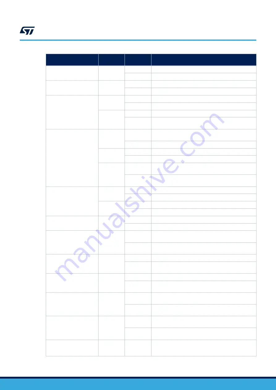
Solder bridge control

Solder

bridge (SB)

State

(1)

Description

(1)

PB6

USART1 TX

SB7

ON

ARD_D1_TX connected to USART1 TX PB6

OFF

ARD_D1_TX not connected to USART1 TX PB6

T_SWO on PB3

SB8

ON

T_SWO connected to PB3

OFF

T_SWO not connected to PB3 and isolated from ARD_D3

PB7

USART1 RX

SB9

ON

ARD_D0_RX connected to USART1 RX PB7

OFF

ARD_D0_RX not connected to USART1 RX PB7

SB10

ON

STLINK_RX (T_VCP_RX) connected to USART1 RX PB7

OFF

STLINK_RX (T_VCP_RX) not connected to USART1 RX
PB7

LSE CLK

selection

SB11

ON

PC14-OSC32_IN connected to ST morpho connector I/O
usage (CN7 pin 25)

OFF

PC14-OSC32_IN not connected to ST morpho connector

SB12 / SB13

ON

LSE provided by external LSE 32.768kHz CLK X2

OFF

LSE not provided by external LSE 32.768kHz CLK X2

SB14

ON

PC15-OSC32_OUT connected to ST morpho connector I/O
usage (CN7 pin 27)

OFF

PC15-OSC32_OUT not connected to ST morpho
connector

B1 User button

SB15

ON

User button connected to PC13

OFF

User button not connected to PC13

SB16

ON

User button connected to PA0

OFF

User button not connected to PA0

SP3T VDD supply

SB18

ON

VDD supplied with FE_CTRL3 (STM32WL IO PC3)

OFF

VDD not connected to FE_CTRL3 (STM32WL IO PC3)

BOOT0/PH3 on STmorpho

connector

SB19

ON

BOOT0/PH3 connected to ST Morpho connector CN7 pin
7

OFF

BOOT0/PH3 not connected to ST Morpho connector CN7 pin
7

32 MHz TCXO supply

SB20

ON

32 MHz TCXO supplied by PB0-VDD_TCXO (to STM32WL)

OFF

32 MHz TCXO disconnected to PB0-VDD_TCXO (to
STM32WL)

VBAT

SB21

ON

VBAT (pin A8 of STM32WL) powered by VDD_SYS

OFF

VBAT (pin A8 of STM32WL) supplied separately (through
VBAT on ST morpho connector CN7 pin 33)

VFBSMPS

SB22

ON

VFBSMPS (pin B2 of STM32WL) connected to
VDDRF1V55 (pin F7 of STM32WL)

OFF

VFBSMPS (pin B2 of STM32WL) disconnected from
VDDRF1V55 (pin F7 of STM32WL) for current probing

VDDSMPS

SB23

ON

VDDSMPS (pin A2 of STM32WL) connected to VDDRF (pin
E8 of STM32WL)

OFF

VDDSMPS (pin A2 of STM32WL) disconnected from VDDRF
(pin E8 of STM32WL) for current probing

VDDA / VREF+ supply

SB24

ON

STM32WL VDDA/VREF+ supplied by VDD_SYS through
SMD ferrite bead L14. Be careful not to provide an
external AVDD supply if SB26 is fitted.

UM2592

Solder bridges

UM2592

 - 

Rev 1

page 30/49

Summary of Contents for NUCLEO-WL55JC STM32WL

Page 1: ...he functionality of the STM32WL Nucleo open development platform with a wide choice of specialized shields The STM32WL Nucleo 64 board does not require any separate probe as it integrates the STLINK V...

Page 2: ...access to all STM32WL I Os Delivered with SMA antenna Flexible power supply options ST LINK USB VBUS or external sources On board STLINK V3 debugger programmer with USB re enumeration capability mass...

Page 3: ...uency band RF frequency range from 433 to 510 MHz 2 1 Codification The meaning of the codification is explained in Table 2 Table 2 Codification explanation NUCLEO WL55JCX Description Example NUCLEO WL...

Page 4: ...Systems IAR Embedded Workbench 1 Keil MDK ARM 1 STMicroelectronics STM32CubeIDE 1 On Windows only 3 3 Demonstration software The demonstration software included in the STM32Cube MCU Package correspond...

Page 5: ...efinition Jumper JPx ON Jumper fitted Jumper JPx OFF Jumper not fitted Jumper JPx 1 2 Jumper fitted between Pin 1 and Pin 2 Solder bridge SBx ON SBx connections closed by 0 resistor Solder bridge SBx...

Page 6: ...ity none 1 stop bit no flow control 4 Press on the B4 Reset button of the STM32WL Nucleo 64 board The STM32WL Nucleo 64 board remains silent until it gets a command from the connected PC to start send...

Page 7: ...source selection JP8 Signals between STLINK V3E and MCU target 1 2 T_SWDIO connected to ST LINK 3 4 T_SWCLK connected to ST LINK 5 6 T_SWO connected to ST LINK 7 8 STLK_VCP_TX connected to ST LINK 9 1...

Page 8: ...re 7 Figure 3 Hardware block diagram STM32WL55 Embedded STLINK V3E CN1 USB Micro B connector B4 RESET button ARDUINO ST morpho GPIO ARDUINO ST morpho 5V PWR SEL DEBUG BOOT0 LED6 COM 32 MHz Crystal or...

Page 9: ...x 16 mm This sticker displays at least the product CPN NUCLEO WL55JCx the board reference MB1389x 0x the FCC ID number YCP MB1389000 the ISED ID 8976A MB1389000 of the board and the CE logo 2 The UID...

Page 10: ...Figure 5 shows both stickers Figure 5 RF certification and UID64 stickers UM2592 PCB layout UM2592 Rev 1 page 10 49...

Page 11: ...Figure 6 Bottom layout UM2592 PCB layout UM2592 Rev 1 page 11 49...

Page 12: ...STLINK V3E supports only SWD and VCP for STM32 devices For information about debugging and programming features of STLINK V3 refer to the user manual STLINK V3SET debugger programmer for STM8 and STM3...

Page 13: ...r STLINK V3E without bridge functions 374F for STLINK V3E with bridge functions 6 3 2 STLINK V3E firmware upgrade The STLINK V3E embeds a firmware upgrade mechanism for the in situ upgrade through the...

Page 14: ...protocol 5 7 GND Ground 6 8 T_SWO T_JTMS target SWO using SWD protocol or Target JTDO using JTAG protocol 7 9 NC Not connected 8 10 T_JTDI T_JTDI not used by SWD protocol Target JTDI using JTAG proto...

Page 15: ...V to 12 V power supply connected to CN7 pin 24 An external E5V 5 V power supply connected to CN7 pin 6 An external 5V_USB_CHGR 5 V USB charger connected to CN1 An external 3V3 3 3 V power supply conne...

Page 16: ...LDO LD1117S50TR U8 VIN 5V AVDD 5V_VIN 3V3 5V_VIN 5V_USB_CHGR 3V3_STLK IOREF E5V VBAT 5V_USB_CHGR VDD_MCU VDD_MCU 3V3 3V3 5V_PWR Power switch 5V 0 5A STMPS2151STR CN5 CN9 CN6 CN8 1 10 1 8 1 6 1 8 CN10...

Page 17: ...ly input from STLINK V3E USB connector with PC 5 V 500 mA maximum If the USB enumeration succeeds the 5V_USB_STLK power is enabled by asserting the T_PWR_EN signal from U9 STLINK V3 STM32F723IEK6 This...

Page 18: ...to power the STM32WL Nucleo 64 board with an external power supply connected to VIN 5 V or 3 3 V External power supply input from VIN 7 V 12 V 800 mA maximum When the STM32WL Nucleo 64 board is power...

Page 19: ...supplied by E5V refer to Table 7 and Figure 13 the jumper configuration must be the following JP4 5 6 jumper E5V Table 7 External power sources E5V 5 V Input power name Connector pins Voltage range Ma...

Page 20: ...leo 64 board is power supplied by a USB charger on CN1 Refer to Table 8 and Figure 14 the jumper configuration must be the following jumper JP2 on pins 7 8 5V_CHGR Table 8 External power sources 5V_CH...

Page 21: ...g to use the 3 3 V CN6 pin 4 or CN7 pin 16 directly as power input refer to Table 9 and Figure 15 In this case the programming and debugging features are not available since the ST LINK is not powered...

Page 22: ...refer to Table 10 and Figure 16 the jumper configuration must be the following Jumper JP4 on pin 9 10 ALONE Table 10 External power sources STD_ALONE_5V Input power name Connector pins Voltage range M...

Page 23: ..._ALONE_5V on connector 11 then the STLINK V3E debugger is not supplied Take care to correctly supply the board when using CN11 Pin 1 of CN11 is the STD_ALONE_5V supply and pin 2 is the GND as shown in...

Page 24: ...board is not power supplied and LED5 remains OFF 6 5 Clock sources 6 5 1 HSE clock high speed external clock There are two ways to configure the pins corresponding to the high speed external clock HS...

Page 25: ...user LED connected to STM32WL I O PB9 To light the LED LED2 a high logic state 1 has to be written in the corresponding GPIO PB9 LED3 USER LED This red LED is a user LED connected to STM32WL I O PB11...

Page 26: ...port switch SP3T to address with the same board the three modes reception high power transmission and low power transmission The choice between the two transmission modes can be done dynamically than...

Page 27: ...WL55JC1 high band frequency ANT SS450 510 from LPRS company for NUCLEO WL55JC2 low band frequency Those antennas have been used for the different FCC ISED CE certifications It is then mandatory to use...

Page 28: ...SB28 must be OFF in this case We can also evaluate the current consumption of the rest of the STM32WL MCU VDD_SYS by connecting an ammeter on JP5 SB27 must be OFF in this case We can also evaluate th...

Page 29: ...rd All the solder bridges present on the STM32WL Nucleo 64 board are used to configure several I Os and power supply pins for compatibility of features and pinout with the target STM32WL supported Tab...

Page 30: ...ser button connected to PA0 OFF User button not connected to PA0 SP3T VDD supply SB18 ON VDD supplied with FE_CTRL3 STM32WL IO PC3 OFF VDD not connected to FE_CTRL3 STM32WL IO PC3 BOOT0 PH3 on STmorph...

Page 31: ...urrent probing SB27 ON VDD_SYS generated from VDD_MCU OFF For I_SYS current probing on JP5 jumper I_RF current probing SB28 ON VDD_RF generated from VDD_MCU OFF For I_RF current probing on JP2 jumper...

Page 32: ...ector CN23 front view Connector Pin number Pin name Signal name STLINK V3EMCU pin Functions CN1 1 VBUS 5V_USB_CHGR 5 V Power 2 DM USB_DEV_HS_CN_N R14 USB differential pair N 3 DP USB_DEV_HS_CN_P R15 U...

Page 33: ...ailable on the STM32WL Nucleo 64 board Figure 22 CN12 SMA connector By default the output of the RF part is on the CN12 SMA connector Table 16 SMA connector pinout Connector Pin number Description CN1...

Page 34: ...UART interface refer to Section 6 6 5 Table 17 ARDUINO connectors pinout Connector Pin number Pin name Signal name STM32 pin 1 Function 1 CN6 1 NC Reserved for test 2 IOREF I O reference 3 NRST T_NRST...

Page 35: ...O D12 ARD_D12 PA6 SPI1_MISO 6 SCK D13 ARD_D13 PA5 SPI1_SCK 7 GND GND 8 AVDD AVDD AVVD VREF Voltage reference 9 SDA D14 ARD_D14 PA11 I2C1_SDA 10 SCL D15 ARD_D15 PA12 I2C1_SCL CN9 1 D7 ARD_D7 PC1 IO 2 P...

Page 36: ...by default to USART1 MCU I O PB6 and PB7 Refer to Section 6 6 5 for details about how to modify the UART interface Table 18 shows the pin assignment of each STM32WL I O on the ST morpho connector Tabl...

Page 37: ...26 NC 25 PB10 26 PB9 27 PC15 28 PB1 27 PB8 28 PB15 29 NC 30 PB2 29 PB5 30 PB11 31 NC 32 PA10 31 PB3 32 AGND 33 VBAT 34 PB4 33 PB12 34 NC 35 NC 36 PB14 35 PB6 PA2 36 PA1 37 NC 38 PB13 37 PB6 PA3 38 PC3...

Page 38: ...Any consequences deriving from such usage will not be at ST charge In no event ST will be liable for any customer usage of these engineering sample tools as reference designs or in production E or ES...

Page 39: ...F Input reference voltage for ADC B6 PC14 OSC32_IN OSC32_IN PC14 LSE_CLK GPIO PC14 B7 VSS GND GND B8 PA13 T_SWDIO T_SWDIO B9 PA11 PA11 ARD_D14 I2C2_SDA C1 PB3 PB3 ARD_D3 TIM2_CH2 T_SWO C2 PB4 PB4 ARD_...

Page 40: ...SSRF VSSRF GND for RF part G8 VSSRF VSSRF GND for RF part G9 OSC_IN OSC_IN HSE CLK H1 PA3 LPUART_RX STLINK_RX T_VCP_RX ARD_D0 H2 PA2 LPUART_TX STLINK_TX T_VCP_TX ARD_D1 H3 PA7 PA7 ARD_D11 TIM17_CH1 SP...

Page 41: ...Reorient or relocate the receiving antenna Increase the separation between the equipment and receiver Connect the equipment into an outlet on circuit different from that to which the receiver is conne...

Page 42: ...operating in conjunction with any other antenna or transmitter Pour satisfaire aux exigences FCC et ISDE concernant l exposition aux champs RF pour les appareils mobiles une distance de s paration de...

Page 43: ...forme la directive 2014 53 UE Le texte complet de la d claration UE de conformit est disponible l adresse internet suivante www st com Bande de fr quence utilis e en transmission et puissance max rayo...

Page 44: ...Revision history Table 20 Document revision history Date Version Changes 17 Nov 2020 1 Initial release UM2592 UM2592 Rev 1 page 44 49...

Page 45: ...3 2 STLINK V3E firmware upgrade 13 6 3 3 Using an external debug tool to program and debug the on board STM32 13 6 4 Power supply 15 6 4 1 Debugging while using VIN or EXT as an external power supply...

Page 46: ...2 Board revision history 38 8 3 Known limitations 38 Appendix A STM32WL Nucleo 64 I O assignment 39 Appendix B Federal Communications Commission FCC and Innovation Science and Economic Development Can...

Page 47: ...l power sources 3V3 21 Table 10 External power sources STD_ALONE_5V 22 Table 11 USART1 connection 28 Table 12 LPUART1 connection 29 Table 13 Solder bridge configuration 29 Table 14 USB Micro B connect...

Page 48: ...7 Figure 12 Power supply input from VIN from 7 V to 12 V 800 mA maximum 19 Figure 13 Power supply input from 5V_EXT 5 V 500 mA maximum 20 Figure 14 Power supply input from ST LINK USB connector with 5...

Page 49: ...ts and ST assumes no liability for application assistance or the design of Purchasers products No license express or implied to any intellectual property right is granted by ST herein Resale of ST pro...

Reviews: