PulseBlaster
I. Introduction
Product Overview
The PulseBlaster
device is an intelligent pulse/pattern generation unit. The intelligence of the
PulseBlaster comes from an imbedded microprogrammed controller core (uPC). The controller is able to
execute instructions that allow it to control program flow. This means that the PulseBlaster understands
Operational Control Codes, Op Codes, and will execute them much the same way as a general-purpose
microprocessor does. The PulseBlaster’s microcontroller is different from the general-purpose
microprocessor in that it does not contain an arithmetic logic unit (ALU) and is incapable of doing
mathematical or logical calculations. However, a unique and distinguishing feature of the PulseBlaster
processor is that the execution time of instructions is user programmable. This feature makes the
PulseBlaster processor capable of executing complex patterns at greatly varying update rates, ranging from
nanoseconds to years per single instruction, with a constant setting accuracy of just one clock period (e.g., a
10 ns setting accuracy at a 100 MHz clock frequency).
Board Architecture
Block Diagram
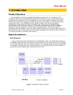
Figure 1 presents the general architecture of the PulseBlaster system. The major building blocks are
the SRAM memory (both internal and external to the processor), the microcontroller (uPC), the integrated
bus controller (IBC), the counter, and the output buffers. The entire logic design, excluding output buffers,
is contained on a single silicon chip, making it a System-on-a-Chip design. User control to the system is
provided through the integrated bus controlled over the PCI bus.
Figure 1:
PulseBlaster board architecture
http://www.spincore.com
5/19/2006
5
PCI Bus


