


XT-P50V
10
10
4-4.
NOTE FOR PRINTED WIRING BOARD AND SCHEMATIC DIAGRAMS
Note on Printed Wiring Board:
•
X
: parts extracted from the component side.
•
Y
: parts extracted from the conductor side.
•
: Pattern from the side which enables seeing.
(The other layers' patterns are not indicated.)
Note on Schematic Diagram:
• All capacitors are in
µ
F unless otherwise noted. pF:
µµ
F
50 WV or less are not indicated except for electrolytics
and tantalums.
• All resistors are in
Ω
and
1
/
4
W or less unless otherwise
specified.
•
C
: panel designation.
•
A
: B+ Line.
•
H
: adjustment for repair.
• Power voltage is dc 14.4V and fed with regulated dc power
supply from BATT and REM (ACC) cord.
• Voltages and waveforms are dc with respect to ground
under no-signal (detuned) conditions.
no mark : TV mode
• Voltages are taken with a VOM (Input impedance 10 M
Ω
).
Voltage variations may be noted due to normal produc-
tion tolerances.
• Waveforms are taken with a oscilloscope.
Voltage variations may be noted due to normal produc-
tion tolerances.
• Circled numbers refer to waveforms.
• Signal path.
E
: AUDIO (TV)
a
: VIDEO (TV)
F
: AUDIO (AUX)
L
: VIDEO (AUX)
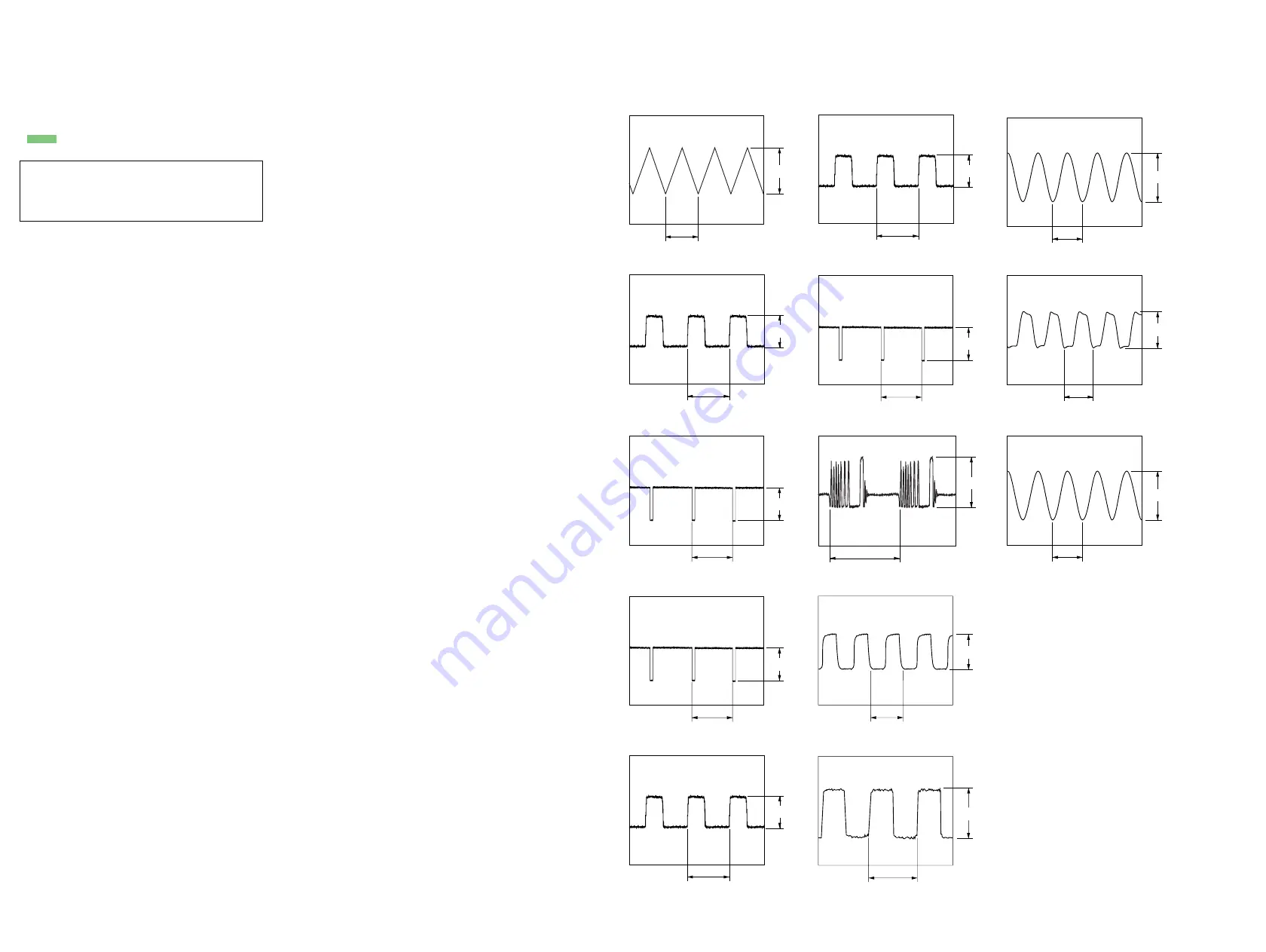
• Waveforms
1
IC100
1
(CT)
2
IC100
7
(OUT1), Q111 (Base)
0.7 Vp-p
4.9
µ
s
3
IC100
q;
(OUT2), Q112 (Base)
13.2 Vp-p
4.8
µ
s
13.4 Vp-p
4.8
µ
s
Caution:
Pattern face side:
Parts on the pattern face side seen from
(Conductor Side)
the pattern face are indicated.
Parts face side:
Parts on the parts face side seen from
(Component Side)
the parts face are indicated.
4
Q112 (Emitter), Q200-1 (Gate)
12 Vp-p
4.8
µ
s
5
Q111 (Emitter), Q200-2 (Gate)
12 Vp-p
4.8
µ
s
6
Q200-1 (Drain)
15 Vp-p
4.8
µ
s
7
Q200-2 (Drain)
14.8 Vp-p
4.8
µ
s
8
IC103
2
(OSC)
36.8 Vp-p
52.5
µ
s
3 Vp-p
226 ns
9
IC110
qj
(OSCIN)
q;
IC113
2
3.4 Vp-p
226 ns
qa
IC113
3
3.6 Vp-p
226 ns
qs
IC113
5
,
6
3.5Vp-p
226 ns
qd
IC108
wd
(XOUT)
5.1 Vp-p
125 ns


