


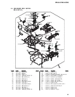
XR-CA370/CA370X
20
20
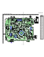
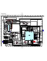
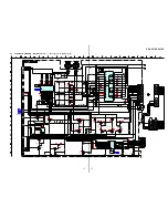
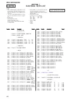
• IC Block Diagrams
– MAIN Board –
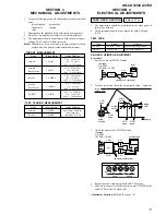
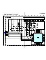
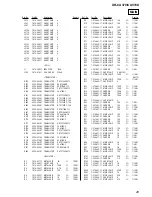
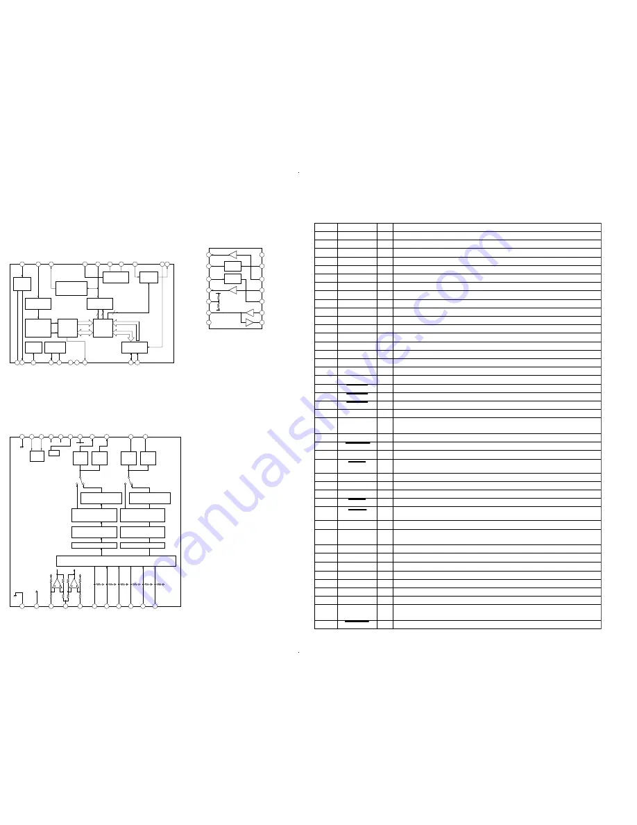
IC200
SAA6588T/V2-518
IC800
MM1175XFF
SCOUT
MRO
MPTH
TCON
OSCO
OSCI
VSSD
VDDD
DAVN
SDA
VREF
MPX
VSSA
VDDA
AFIN
MAD
PSWN
SCL
2
1
6
15
11
13
16
14
12
INTERFACE
REGISTER
SIGNAL QUALITY
DECODER
CLOCKED
COMPARATOR
POWER SUPPLY
& RESET
TEST
CONTROL
OSCILLATOR
& CLOCK
PAUSE
DETECTOR
MULTI
PATH
DETECTOR
57kHz
8th ORDER
BAND-PASS FILTER
RDS/RDBS
DECODER
RDS/RDBS
DEMODULATOR
IIC BUS SLAVE
TRANSCEIVER
17
18
CIN
19
LVIN
20
8
7
DATA
CLOCK
DATA
CLOCK
4
4
5
9
10
3
4
5
RESET
SWITCH
BATT
SWITCH
1
2
3
4
5
6
7
8
9
10
14
13
12
11
BUS ON
OUT
RESET
OUT
BATT
CLK
OUT
VREF
DATA
IN/OUT
GND
BATT
CHECK
CLK
IN
BUS ON
IN
RESET
IN
VCC
DATA IN
DATA OUT
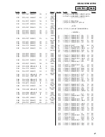
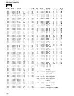
IC400
BD3803F-FE2
22
DGND
21
SDA
20
SCL
19
MUTE
18
SEL
17
ADJ
16
VCC
15
OUTF1
14
OUTR1
13
OUTF2
12
OUTR2
6
B1
7
B2
8
C1
9
C2
10
D1
11
D2
1
2
C BUS
LOGIC
VCO
FADER
(0
∼
–58,
–
∞
dB)
FADER
(0
∼
–58,
–
∞
dB)
FADER
(0
∼
–58,
–
∞
dB)
FADER
(0
∼
–58,
–
∞
dB)
BASS, TREBLE, MIDDLE
(–15dB
∼
+15dB, 1dB STEP)
VOLUME
(+23
∼
–79dB, –
∞
dB
1dB STEP)
INPUT GAIN
(0
∼
15dB, 1dB STEP)
MUTE
INPUT SELECTOR
(4 STEREO INCLUDE 1 ISOLATION INPUT)
BASS, TREBLE, MIDDLE
(–15dB
∼
+15dB, 1dB STEP)
VOLUME
(+23
∼
–79dB, –
∞
dB
1dB STEP)
INPUT GAIN
(0
∼
15dB, 1dB STEP)
MUTE
1
A
GND
2
VCC/2
FIL
3
AP1
4
AN
5
AP2
TONE
PASS
TONE
PASS
5-7.
IC PIN FUNCTION DESCRIPTION
•
MAIN BOARD IC1 MN101C49KSF (SYSTEM CONTROLLER)
Pin No.
Pin Name
I/O
Description
1
VREF –
—
Reference voltage (0V) terminal (for A/D converter)
2
VSM
I
FM and AM signal meter voltage detection input from the tuner unit (A/D input)
3 to 6
NC
I
Not used
7
QUALITY
I
Noise level detection signal input from the tuner unit (A/D input)
8
MPTH
I
Multi-path detection signal input from the RDS decoder (A/D input)
9
NC
I
Not used
10
VREF +
—
Reference voltage (+5V) terminal (for A/D converter)
11
VDD
—
Power supply terminal (+5V)
12
OSC2
O
Main system clock output terminal (18.432 MHz)
13
OSC1
I
Main system clock input terminal (18.432 MHz)
14
VSS
—
Ground terminal
15
XI
I
Sub system clock input terminal (32.768 kHz)
16
XO
O
Sub system clock output terminal (32.768 kHz)
17
MMOD
I
Setting terminal for the single chip mode “L”: single chip (fixed at “L” in this set)
18
LCD-SO (TX)
O
LCD serial data output to the liquid crystal display driver
19
LCD-SI (RX)
I
LCD serial data input from the liquid crystal display driver
20
LCD-CKO
O
LCD serial transfer clock signal output to the liquid crystal display driver
21 to 23
NC
O
Not used
24
SYS-RES
O
System reset signal output to the SONY bus interface “L”: reset
25
BUS-ON
O
Bus interface control signal output to the SONY bus interface “L”: uni-link on
26
KEYACK
I
Key acknowledge signal detection input from the liquid crystal display driver
27
DAVN
I
RDS serial data request signal input terminal
28
BU-IN
I
Battery detection signal input from the bus interface and battery detect circuit
“L” is input at low voltage
29
NC
I
Not used
30
TU-ATTIN
I
Tuner muting on/off control signal input from the tuner unit “L”: muting on
31, 32
NC
I
Not used
33
RESET
I
System reset signal input from the reset signal generator and reset switch “L”: reset
“L”is input for several 100 msec after power on, then it changes to “H”
34
NC
O
Not used
35
BEEP
O
Beep sound drive signal output to the power amplifier “H”: beep on
36
POWER-ON
O
Main system power supply on/off control signal output “H”: power on
37
ILL-IN
I
Illuminate line detection signal input terminal “L”: ill on Not used
38
ACC-IN
I
Accessory detection signal input “L”: accessory on
“H” is input for several 200 msec after accessory on, then it changes to “L”
39
NC
O
Not used
40
TEL-ATT
I
Telephone muting signal input terminal At input of “H”, the signal is attenuated by –20 dB
Not used
41
NCI
I
Not used
42
BUS-SO
O
Serial data output to the SONY bus interface
43
BUS-SI
I
Serial data input from the SONY bus interface
44
BUS-CKO
O
Serial data transfer clock signal output to the SONY bus interface
45
I2C-SIO
I/O
Two-way data bus with the tuner unit, RDS decoder and electrical volume
46
NC
O
Not used
47
I2C-CKO
O
Serial data transfer clock signal output to the tuner unit, RDS decoder and electrical volume
48
AMP-ON
O
Standby on/off control signal output to the power amplifier
“L”: standby mode, “H”: amplifier on
49
AMP-ATT
O
Muting on/off control signal output to the power amplifier “L”: muting on


