35
•
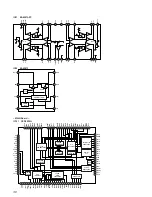
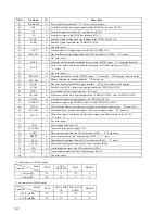
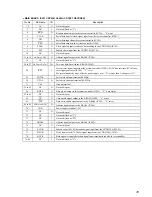
MAIN BOARD IC501 CXP83413-049Q (CD TEXT DECODER)
Pin No.
Pin Name
I/O
Description
1, 2
NC
O
Not used (open)
3
NC
I
Not used (fixed at “L”)
4
REQ
O
Request signal output to the system controller (IC201) “L” active
5
CCLK
I
Serial data transfer clock signal input from the system controller (IC201)
6
CSI
I
Serial data input from the system controller (IC201)
7
CSO
O
Serial data output to the system controller (IC201)
8
SCLK
O
Clock signal output for subcode data reading to the CXD2530Q (IC101)
9
SSI
I
Subcode data input from the CXD2530Q (IC101)
10
NC
O
Not used (open)
11 to 18
ADD0 to ADD7
O
Address signal output to the S-RAM (IC502)
19
NC
I
Not used (fixed at “L”)
20 to 27
DATA0 to DATA7
I/O
Two-way data bus with the S-RAM (IC502)
28
RST
I
System reset signal input from the system controller (IC201), SONY bus interface (IC302) and
reset signal generator (IC304) “L”: reset
For several hundreds msec. after the power supply rises, “L” is input, then it changes to “H”
29
EXTAL
I
System clock input terminal (10 MHz)
30
XTAL
O
System clock output terminal (10 MHz)
31
VSS
—
Ground terminal
32 to 55
NC
O
Not used (open)
56
BUSY
O
Busy signal output to the system controller (IC201) “L”: busy status
57 to 61
NC
O
Not used (open)
62
CE
O
Chip enable signal output to the S-RAM (IC502) “L” active
63
WE
O
Data write enable signal output to the S-RAM (IC502) “L” active
64 to 69
ADD8 to ADD13
O
Address signal output to the S-RAM (IC502)
70
VDD
—
Power supply terminal (+5V)
71
NC
O
Not used (open)
72
NC
I
Not used (fixed at “L”)
73
NC
I
Not used (fixed at “H”)
74
ADD14
O
Address signal output to the S-RAM (IC502)
75
NC
O
Not used (open)
76
SCOR
I
Subcode sync (S0+S1) detection signal input from the CXD2530Q (IC101)
77
WFCK
I
Write frame clock (7.35 kHz) signal input from the CXD2530Q (IC101)
78
BUCK
I
Backup power supply detection signal input terminal (used also to reset standby)
79, 80
NC
I
Not used (fixed at “L”)
Summary of Contents for Xplod CDX-737
Page 4: ...4 4 ...

