background image

26

MZ-NF610

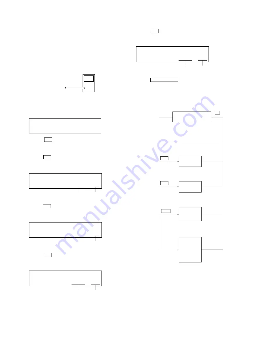
Laser Power Check

Note:

If result of measurement of the laser power does not satisfy the
specification, either replace the OP (optical pick-up unit) or check
whether the laser circuit block is working correctly.
When the result of laser power measurement does not satisfy the
specification even though the laser circuit block is confirmed to be
working correctly, replace the OP (optical pick-up unit).

• Connection

• Checking method

1. Select the manual mode of test mode (see page 14), and set the

laser power checking mode (item number 010).

2. Press the 

.

key continuously until the optical pick-up

moves to the most inward track.

3. Open the cover and set the laser power meter on the objective

lens of the optical pick-up.

4. Press the 

>

  key,  and set the laser MO read check mode

(item number 011).

5. Check that the laser power meter reading is 0.800 ± 0.10 mW.
6. Press the

>

key, and set the laser CD read check mode (item

number 012).

7. Check that the laser power meter reading is 0.910 ± 0.11 mW.
8. Press the

>

key,  and set the laser MO (X2 speed) write

check mode (item number 013).

9. Check that the laser power meter reading is 4.95 ± 0.59 mW.

10. Press the

>

    key,  and set the laser MO (X4 speed) write

check mode (item number 014).

11. Check that the laser power meter reading is 5.93 ± 0.71mW.
12. Press the

x

CANCEL/

CHG

key to quit the manual mode, and

activate the test mode (display check mode).

Overall Adjustment Mode

• Configuration of Overall Adjustment Mode

 0 10      

L a s e r

Set LCD display

Set LCD display

# # # S * *

 0 11

address

adjusted value

laser

power meter

optical pick-up

objective lens

Set LCD display

# # # S * *

 0 12

address

adjusted value

Set LCD display

# # # S * *

 0 13

address

adjusted value

Set LCD display

# # # S * *

 0 14

address

adjusted value

VOL+


key

 key

 key


 key

Overall adjustment mode

(Title display)

Continuing
overall adjustment

[END SEARCH]

   key

Electrical

offset

adjustment

MO overall
adjustment

CD overall

adjustment

Temperature

correction

and

Power supply

adjustment

auto item feed

Summary of Contents for Walkman MZ-NF610

Page 1: ...s a trademark of Apple Computer Inc in the United States and or other countries MMX and Pentium are trademarks or registered trademarks of Intel Corporation All other trademarks and registered trademarks are trademarks or registered trademarks of their respective holders and marks are omitted in this manual MD recorder Audio playing system MiniDisc digital audio system Laser diode properties Mater...

Page 2: ...battery NH 7WMAA 1 2V 700 mAh MIN Ni MH LR6 size AA alkaline battery Dimensions Approx 81 0 27 7 74 4 mm w h d 31 4 11 8 3 in Mass Supplied accessories Approx 103 g 3 6 oz the recorder only 1 The LINE IN OPTICAL jack is used to connect either a digital optical cable or a line analog cable 2 The i jack connects either headphones earphones or a line cable 3 Measured in accordance with JEITA US and f...

Page 3: ...Board 4 4 46 6 9 IC Pin Function Description 52 7 EXPLODED VIEWS 7 1 Case Section 58 7 2 Chassis Section 59 7 3 MAIN Board Section 60 7 4 Mechanism Deck Section 1 MT MZN710 177 61 7 5 Mechanism Deck Section 2 MT MZN710 177 62 8 ELECTRICAL PARTS LIST 63 CAUTION Use of controls or adjustments or performance of procedures other than those specified herein may result in hazardous ra diation exposure N...

Page 4: ...r Professional Windows 2000 versions other than Professional Windows 98 versions other than Second Edition Windows NT Windows 95 Personally constructed PCs or operating systems An environment that is an upgrade of the original manufacturer installed operating system Multi boot environment Multi monitor environment Notes We do not ensure trouble free operation on all computers that satisfy the syst...

Page 5: ...by mode I Battery indication Shows approximate battery condition J Indication for remaining playing time of the current track or of the disc Indication for remaining recordable time of the disc K Time display L Character information display Displays the disc and track names error messages track numbers etc M Play mode indications Shows the play mode shuffle play repeat play group play bookmark pla...

Page 6: ...MAIN BOARD In order to remove mechanism deck please remove MAIN board and upper panel section OP SERVICE ASSY LCX 5R HOLDER ASSY DC MOTOR SLED M602 DC MOTOR OVER WRITE HEAD UP DOWN M603 DC SSM18B MOTOR SPINDLE M601 SET SECTION 3 DISASSEMBLY This set can be disassembled in the order shown below 3 1 Disassembly Flow ...

Page 7: ...ction 1 two screws M1 4 2 two screws M1 4 3 Remove the case lower in the direction of the arrow 5 torsion spring pop up L 3 two step screws 2 Slide the open slider in the direction of the arrow and open the upper panel section set chassis assy torsion spring pop up L 1 flexible board CN871 4 upper panel section ...

Page 8: ...position of both switch and knob hold 5 button control 4 open locker knob hold switch case upper sub assy 8 MAIN board 6 battery terminal 5 battery terminal board 2 flexible board motor CN701 3 flexible board CN871 7 flexible board optical pick up CN501 1 Remove two solders of the flexible board over write head 4 four screws M1 4 ...

Page 9: ...k MT MZN710 177 3 7 Set Chassis Assy The portion which projected is removed 1 two step screws MD 3 mechanism deck MT MZN710 177 2 2 two screws TP 1 7 2 5 5 set chassis assy 4 ground spring USB 1 tension spring lock 3 battery case ...

Page 10: ...5 screw M1 4 6 thrust detent spring 8 Pull off lead screw 7 over write head section OP service assy LCX 5R 9 Opening the over write head toward the direction A remove the OP service assy LCX 5R toward the direction B A B Note Do not open the entire assy forcibly when opening the over write head ...

Page 11: ...Holder Assy 3 10 DC Motor Sled M602 4 holder assy 3 boss 3 boss 1 convex portion 2 Open the holder assy 2 washer 0 8 2 5 5 DC motor sled M602 4 two screws M1 4 3 gear SA 1 Remove six solders of the motor flexible board ...

Page 12: ... tapping screws 2 tapping screw 3 motor cover 6 gear HA 4 gear HB 5 gear HC DC motor over write head up down M603 3 15 mm gear HA Note Press fit the gear HA up to the position of the DC motor over write head up down M603 as shown below 7 DC motor over write head up down M603 1 Remove six solders of the motor flexible board ...

Page 13: ...mode the disc is discriminated be tween CD and MO and each adjustment is automatically ex ecuted in order If a fault is found the system displays its loca tion Also the manual mode allows each individual adjustment to be automatically adjusted Operation in the test mode is performed with the set A key having no particular description in the text indicates a set key Setting Method of Test Mode Ther...

Page 14: ...und Skip Check Result Display Mode Key Check Mode Test Mode Display Check Mode Press the xCANCEL CHG key Press the key or press the VOL key on the remote commander Press the ENTER N or VOL key Press the key or press the VOL key on the remote commander Electrical Offset Adjustment Power Supply Adjustment Auto Item Feed CD Overall Adjustment MO Overall Adjustment Self Diagnosis Result Display Mode P...

Page 15: ...ich if an error occurred during the recording or playing the mechanism control block and the power supply control block in the microcomputer detect it and record its cause as history in the nonvolatile memory By checking this history in the test mode you can analyze a fault and determine its location Total recording time is recorded as a guideline of how long the optical pick up has been used and ...

Page 16: ...error 00 No error No error 01 Illegal access target Adrs Attempt to access an abnormal address address was specified Servo system error 02 High temperature Temp High temperature detected 03 Focus error Fcus Disordered focus or can not read an address 04 Spindle error Spdl Abnormal rotation of disc 11 TOC error TOC Faulty TOC contents TOC error 12 Data reading error Data data could not be read at S...

Page 17: ...he test mode see page 13 2 Press the ENTERN key or VOL key and the playing or recording sound skip result display mode becomes active re spectively where the LCD displays the following 3 When the ENTERN key is pressed total error count is dis played on the LCD and each time the key is pressed the display item moves down by one as shown below Also if the key is pressed the display item moves up by ...

Page 18: ...own Example1 When the keys on the set are considered as OK Example2 When the keys on the remote commander are con sidered as OK 5 When all keys were checked or if the upper panel is opened the key check mode quits and the test mode display check mode comes back 8 88 S E T O K Set LCD display 8 88 R M C O K Set LCD display ...

Page 19: ...aptor is used Note2 Power supply adjustment auto item feed mode page 25 is available to perform the temperature Correction and Power Supply Adjustment without entering the manual mode NV Reset Setting Method of NV Reset 1 Select the manual mode of the test mode and set item number 021 NV Reset see page 14 2 Press the X key SECTION 5 ELECTRICAL ADJUSTMENTS Outline In this set automatic adjustment o...

Page 20: ...the TP1928 VCO1 on the MAIN board and adjust VOL key voltage up or VOL key volt age down so that the voltage becomes 2 35 0 05V 2 Press the X key on the set or the key on the remote commander to write the adjusted value Adjustment and Connection Location MAIN board see page 24 Adjustment Method of VC1_HIGH REC item number 742 1 Connect a digital voltmeter to the TP1928 VCO1 on the MAIN board and a...

Page 21: ...LCD display digital voltmeter TP1907 REGO3 TP1311 GND MAIN board 7 47 A D Adjusted value Set LCD display Adjustment Method of REG3_LOW2 item number 748 1 Connect a digital voltmeter to the TP1907 REGO3 on the MAIN board and adjust VOL key voltage up or VOL key voltage down so that the voltage becomes 1 25 0 01V 2 Press the X key on the set or the key on the remote commander to write the adjusted v...

Page 22: ...theTP1620 VREC on the MAIN board and adjust VOL key voltage up or VOL key voltage down so that the voltage becomes between 1 65V and 1 75V 2 Press the X key on the set or the key on the remote commander to write the adjusted value Adjustment and Connection Location MAIN board see page 24 Adjustment Method of CHGV_LOW item number 755 Note Remove the rechargeable battery 1 Connect a digital voltmete...

Page 23: ...voltage becomes 1 41 0 015V 2 Press the X key on the set or the key on the remote commander to write the adjusted value Adjustment and Connection Location MAIN board see page 24 Adjustment Method of CHGI_HIGH Charge current item number 758 Note Remove the rechargeable battery Connect the resistor 10 0 5 between terminals of BATT and BATT 1 Connect a digital voltmeter to the BATT and BATT on the MA...

Page 24: ...845 TP1837 TP1835 TP1896 TP1807 TP1736 TP1721 TP1716 TP1719 TP1724 TP1725 TP1855 TP1870 TP1861 TP1860 TP1722 TP1713 TP1858 TP1718 TP1717 TP1715 TP1714 TP1711 TP1712 TP1898 TP1857 TP1867 TP1720 TP1805 TP1854 TP1823 TP1852 TP1850 TP1897 TP1806 TP1723 SL502 TP1961 TP1966 TP1967 TP1847 TP1529 TP1523 TP824 TP1528 TP1833 TP1834 TP1830 TP1831 TP1868 TP1511 TP1510 TP1525 TP1536 C825 C826 SL802 1 15 1 6 7 ...

Page 25: ...y 7 41 V C 1 L Set LCD display 0 00 A D J O K Set LCD display key key key key key key key key key key END SEARCH key 000Assy 015 SetTmp 741 VC1 L 742 VC1 H 743 VC2 Lo 744 VC2 Hi 745 REG1 key key key key key key key key key 752 VREC M 753 VREC H 755 ChgV L 756 ChgV H key key 757 CIL key key 758 CIH 000 ADJ OK key key key key 747 REG3L1 748 REG3L2 key key 749 REG3 H 751 VREC L key key 5 Connect a di...

Page 26: ...and set the laser CD read check mode item number 012 7 Check that the laser power meter reading is 0 910 0 11 mW 8 Press the key and set the laser MO X2 speed write check mode item number 013 9 Check that the laser power meter reading is 4 95 0 59 mW 10 Press the key and set the laser MO X4 speed write check mode item number 014 11 Check that the laser power meter reading is 5 93 0 71mW 12 Press t...

Page 27: ... adjustment information F MO overall adjustment completed 1 Manual adjustment exists overall adj not completed 0 Not adjusted Right side CD overall adjustment information F CD overall adjustment completed 1 Manual adjustment exists overall adj not completed 0 Not adjusted Set LCD display Note Adjust the CD first when performing adjustment ...

Page 28: ...wing message will be displayed if adjustment procedure is mistaken in the CD and MO overall adjustment Message Display timing During CD MO DISC CLOSE automatic distinction overall adjustment During MO DISC Set CD automatic distinction overall adjustment During offset adjustment Set MO During offset adjustment During CD MO DISC NoTmp automatic distinction overall adjustment During CD MO DISC NoChg ...

Page 29: ... HPIT setting servo OFF 2 MO overall adjustment items Item No Description 716 VC VR power supply H L selection 100 R_GRV setting servo OFF Low reflection electrical offset adjustment 112 Laser ON Focus UP vc correction ALFA offset adjustment 113 IJ offset adjustment 114 FE offset adjustment 118 Wpp denominator offset adjustment LPIT adjustment 200 LPIT setting servo OFF 561 SLED inward movement 22...

Page 30: ...ear Setting Method 1 Select the manual mode of the test mode and set item number 043 see page 14 2 Press the X key 3 Press the xCANCEL CHG key to return to the test mode dis play check mode 0 43 R e s Set LCD display 0 43 R e s C l r r Resume clear complete 0 43 S 0 0 Address Set LCD display ...

Page 31: ...ver has been installed For further information see System requirements page 4 in SECTION 1 SERVICING NOTES 3 Application USB_PatchWriter for patch data rewriting How to Get the Application USB_PatchWriter for Patch Data Rewriting Contact our service technical support division to get the application Pre check 1 Check the microcomputer version in this set For a checking method of the microcomputer v...

Page 32: ...utton The patch data writing and the verify processing will be executed automatically in the following order 1 Writing to patch area front area 2 Writing to patch area reverse area 3 Verifying patch area front area 4 Verifying patch area reverse area 7 The operation will terminate with the a blue mark given to all areas If the red mark is given to any area the nonvolatile memory will be faulty ...

Page 33: ...ton to confirm the contents of the patch data rewrited 2 The application reads out the front and reverse patch areas and displays the results in the edit box Confirm that the upper column coincides with the lower column as the following window 3 Click the OK button to close the window ...

Page 34: ...irmation Note When the following procedure is not completed but USB cable is extracted the application does not recognize the set at exchanging of the set 1 Click the USB DISCONNECT button 2 Confirm that You can change another device is displayed in the message block 3 Disconnect the USB cable from the personal computer and the set ...

Page 35: ...page 4 in SECTION 1 SERVICING NOTES 3 Application NVWriter for NV values rewriting How to get the application NVWriter for NV values rewriting Contact our service technical support division to get the application Pre check 1 Check the microcomputer version in this set For a checking method of the microcomputer version see SECTION 4 TEST MODE page 13 2 Check that the Net MD Driver has been installe...

Page 36: ...to Servo 1 area front area 2 Writing to Servo 1 area reverse area 3 Writing to Power Supply 1 area front area 4 Writing to Power Supply 1 area reverse area 5 Writing to Power Supply 2 area front area 6 Writing to Power Supply 2 area reverse area 7 Verifying to Servo 1 area front area 8 Verifying to Servo 1 area reverse area 9 Verifying to Power Supply 1 area front area 10 Verifying to Power Supply...

Page 37: ...37 MZ NF610 7 The operation will terminate with Compere OK given to all areas If Compere NG is given to any area the nonvolatile memory will be faulty 8 Click the USB DISCONNECT button ...

Page 38: ...38 MZ NF610 9 Confirm that the window becomes as shown below where the Write Verify button is inactive 10 Disconnect the USB cable from the personal computer and the set ...

Page 39: ...EN CLOSE SW 93 S801 HALF LOCK S803 OPEN CLOSE PROTECT 89 S806 PROTECT OSCI 1 OSCO 2 UOSCI 179 UOSCO 180 X803 22 5792MHz X802 48MHz HALF LOCK 33 HA 35 HB SWITCH Q604 605 A B 38 OUT B 41 OUT A ANALOG IN RESET Q871 REGO1 UNREG DO 4 EEPROM IC852 DI 3 XSK 12 2 XCS 1 CDTI 13 A D CONV IC302 CCLK 14 STDO 9 BCLK 10 MCLK 11 LRCK 12 CSN 15 PDN 16 3 L IN 4 R IN 146 VREC PWM EFM 7 71 EFMO 42 VREC IN1 37 VREC I...

Page 40: ... the parts face side seen from Side B the parts face are indicated MAIN board is four layer printed board However the patterns of layers 2 and 3 have not been included in this diagrams surface Lead layout of conventional IC CSP chip size package Replacement of IC501 IC801 on MAIN board requires a special tool The voltage and waveform of CSP chip size package cannot be measured because its lead lay...

Page 41: ...DD VB DTCK KEY_R RADIO_ON RGND J303 2 2 1 TO SIDE B 1 686 317 11 11 C708 R840 1 2 A B C D E F G H I 3 4 5 6 7 8 9 10 11 6 3 Printed Wiring Board MAIN Board Side A Uses unleaded solder Semiconductor Location Ref No Location D606 H 4 D607 H 3 D653 H 2 D654 H 2 D953 H 8 D958 I 8 IC302 E 9 IC701 D 5 Q501 F 7 Q603 H 4 Q604 H 4 Q605 H 3 Q652 H 2 Q654 H 3 Q672 B 9 Q955 I 7 ...

Page 42: ...25 TP1536 C825 C826 SL802 S806 PROTECT OPTICAL LINE IN JACK 1 2 J303 1 2 1 TO SIDE A SWITCH LCD MODULE 1 15 DC IN 3V J951 OVER WRITE HEAD 1 6 7 13 18 19 24 12 CSP Chip Size Package CSP Chip Size Package 1 3 4 5 RECHARGEABLE BATTERY NH 7WMAA 1 2V OR DRY BATTERY SIZE AA IEC DESIGNATION LR6 1 5V 1 M 10 U U N V W N V W M602 SLED M601 SPINDLE M603 OVER WRITE HEAD UP DOWN 1 686 317 11 11 1 16 17 32 33 4...

Page 43: ...D901 C907 C914 R926 D902 TP1924 C913 C911 R903 R901 C901 TP926 R933 R934 TP927 TP1928 R932 D952 R617 Q672 R672 R674 TP1958 R976 R975 Q953 R963 D955 R967 R919 R914 C926 C631 R659 R654 C952 C630 44 C615 C616 J951 CN651 C626 C614 R908 IC951 IC901 XPC18A22AEPR2 CPH5614 MCH6616 TL E TS8K1TB 10 6 3V 47 4V 10 6 3V UN9115J TX SO 47 10V FMMT617TA 22 6 3V XP151A12A2MR DF3A6 8FE TPL3 220 6 3V 220 4V 100 6 3V...

Page 44: ...6 TP1727 TP1736 TP1737 TP1713 TP1714 TP1715 TP1716 TP1717 TP1718 TP1719 TP1720 TP1721 TP1722 TP1723 TP1712 TP1711 C718 C720 C719 C721 C715 C716 TP1724 TP1725 C705 C703 C701 TP1701 TP1702 TP1703 TP1704 C712 C710 C708 C706 C704 C702 TP1710 TP1709 TP1708 TP1707 TP1705 TP1706 TP1739 TP1524 TP1535 TP1519 TP1548 C517 CN701 CN501 U V V U W N R701 R703 IC501 SN761058AZQLR 0 047 B 4700p B 4700p B 0 01 B 0 ...

Page 45: ...807 TP1806 TP1805 TP1804 TP1803 TP1802 TP1801 TP1823 TP1822 TP1821 R844 FB805 FB804 FB803 R832 R831 R830 TP1870 R813 R811 R807 R808 R806 R809 X801 R814 R815 R805 TP1898 TP1820 C833 TP896 TP897 C807 R840 TP1857 TP1868 C843 C842 TP1867 IC801 L802 C806 R804 R803 C805 L803 C834 R817 C815 R816 C811 FB801 R818 C812 C813 C814 R819 R820 C820 C822 C823 R835 R834 R836 FB802 X802 1000p B 0 1 0 1 B 0 047 B 0 ...

Page 46: ...P1880 C310 R848 C306 C204 C104 R202 C325 C314 C313 C205 C315 C364 C162 FB301 R874 R106 J303 HP OUT TP1882 TP1883 TP1884 TP1885 TP1886 TP1887 TP1888 TP1889 TP1890 TP1891 TP1892 TP1893 TP1894 TP1895 CN871 R201 R101 F301 IC361 10 4V 220 4V 220 4V 2SC4738FL 10 6 3V NNCD6 8H T1 22k 0 5 1k 1k 100 1k 100k 10k 1M 0 0 XP1501 TXE 220k 470k 100k 0 100k 1k 1k 0 2 2 B 0 22 B 10 0 22 B 0 1 F 10 10k 10k 10k 10k ...

Page 47: ... CDTI 11 MCLK 10 BCLK 9 STDD 12 LRCK IPGA IC Block Diagrams IC302 AK5354VT E2 IC361 TA2131FL EL V REF MT SW BST SW BEEP 19 20 21 22 23 24 18 17 16 15 14 13 PW SW 12 11 10 8 7 BST1 9 BST2 6 5 4 3 2 1 BST AGC PW B PW A ADD TC MT VCC INR INL BEEP OUTB BEEP OUTA B OUT_L PWR GND OUT_R DET AGC IN BST NF2 LPF2 NF1 LPF1 VREF VREF IN GND BEEP IN BST SW MUTE STB ...

Page 48: ...TM 47 46 45 42 FE 41 ABCD 40 RFI 39 ASSY 37 EFMO DGND RESET 34 VGIN 33 SBUS 32 SCK CPOUT CP DVCC IY JY JX AVCC AVCC C B A D PEAK BOTM TON C OFTRK NPPO TE 44 43 15 16 17 18 19 20 21 22 23 24 25 26 27 28 31 30 29 35 36 38 CIG ABCD T ON EFM COMP SERIAL I F POWER SUPPLY SIGNAL MONITOR OFTRK FE TPP WPP RF A B C D I J NPP TON CSL AW DW TONE PEAK TON BOTM ADIP TE TWP P PK BTM AW CSLO VREF A C D C OFTTH P...

Page 49: ...HB VG VRECIN2 OUTB PGND2 PGND2 OUTA VRECIN1 OUTPUT SW CONTROL OUTPUT SW CONTROL PWM SYSTEM OUTPUT SW CHARGE CONTROL DC IN DETECT DC IN BANDGAP HI BRIDGE PRE DRIVER EFM PRE DRIVER CHARGE PUMP 2 CHARGE PUMP 1 VREF BUFFER SET UP DOWN PRE DRIVER LEVEL SHIFT VC AMP CHARGE MONITOR X2 X4 BATTERY CHARGER REGULATOR VC VG DC IN DC IN DC IN DC IN DC IN VIO VIO VC VC VC VC VC2 VC2 VG VC VG VG2 SW VG2 VG3 VG3 ...

Page 50: ...32 33 34 35 UO2 VMU2 VMR2 RO2 PGND2 FO2 VMF2 VI1 WI1 PGNDW1 WO1 WMVW1 VO1 PGNDUV1 UO1 VMU1 VMR1 RO1 PGND1 FO1 VMF1 19 18 17 16 15 FI1 RI1 COM1 CPUI1 CPVI1 22 21 20 CPWI1 GND2 NC BIAS VC ROE VC 3Phase control ch1 3Phase control ch2 3Phase Pre driver ch1 H BRIDGE PRE DRIVER CH1 H BRIDGE CONTROL CH1 VC VC VG VC VG VC VC OE VG VG VCVG VCVG GND VG VC VG VC VG VC VG VC VC VC U V W U V W H BRIDGE CONTROL...

Page 51: ...27 CRST2 28 DTC2 29 INM2 30 31 RF2 32 VC2G 7 LVB 8 HVB 9 VSTB 10 VC1 11 VCO1 48 VREF 47 REGC3 46 REGC2 45 REGC1 44 REGI1 43 REGO1 37 VCOUT 36 VO2 35 L2 34 L2 33 PGND2 42 VC2 41 REGO2 40 REGI3 39 REGO3 38 CVIN 64 SLEEP 63 CLK 62 SEQSEL 61 WDT 60 SCK 59 STRB 58 DATA 57 HPI2 56 HPI1 55 MUTEON 54 GND 53 VHP1 52 HP1 L CH 51 PGND4 50 HP2 R CH 49 VHP2 PWM START UP SET UP DC DC CONVERTOR SET UP PRE DRIVER...

Page 52: ...Middle point voltage input from the RF amplifier Monitor output terminal of A D converter input signal Not used open The lower limit voltage of A D converter input terminal connected to the ground Sled error signal input from the RF amplifier Tracking error signal input from the RF amplifier Auxiliary A D input fixed at H in this set The upper limit voltage of A D converter input terminal fixed at...

Page 53: ...class headphone amplifier Not used open PWM modulator signal output for the D class headphone amplifier Not used open TigerI F data 0 to 7 terminal Not used open TigerI F REQUEST terminal Not used connected to the ground TigerI F ACK terminal Not used connected to the ground Pause key detection input terminal from the switch liquid crystal display module Detection signal input terminal of the reco...

Page 54: ... supply AC adaptor charging stand detection signal input HOLD switch input terminal L hold ON Traverse count measurement monitor input A D terminal of the battery charge contro IC output selection signal output Charge discharge changeover control signal output for the current sense amplifier DC plug detection signal input Not used open Spindle servo monitor signal input Chip select signal output t...

Page 55: ...minal for the USB oscillation circuit Resonator 48MHz connection terminal for the USB oscillation circuit Not used connected to the ground Not used open Not used open Not used connected to the ground Not used open Not used open Power supply control signal output to the RF amplifier Not used open Power supply control signal output to the liquid crystal display module Not used open Built in speaker ...

Page 56: ...ly terminal for the microcomputer I F block Ground terminal for the microcomputer I F block Power supply terminal for the microcomputer I F block Ground terminal for the microcomputer I F block Power supply terminal for the microcomputer I F block Ground terminal for the microcomputer I F block Power supply terminal for the microcomputer analog Ground terminal for the microcomputer analog Power su...

Page 57: ...6 to 312 I O Pin Name FVDD0 FVSS0 DVDD5 6 DRAMVDD3 4 MSAK NC Description Power supply terminal for the built in flash memory Ground terminal for the built in flash memory Power supply terminal Power supply terminal for DRAM Not used open Not used open ...

Page 58: ... 529 01 SCREW STEP 4 3 246 238 01 BUTTON CONTROL 5 3 237 097 01 LOCKER OPEN 6 3 375 114 71 SCREW 7 1 804 989 11 LCD MODULE The components identified by mark 0 or dotted line with mark 0 are critical for safety Replace only with part number specified Les composants identifiés par une marque 0 sont critiques pour la sécurité Ne les remplacer que par une pièce portant le numéro spécifié chassis secti...

Page 59: ...60 61 55 51 3 237 072 01 SCREW MD STEP 53 X 3382 628 1 CHASSIS ASSY SET 54 3 249 532 01 SPRING POP UP L TORSION 55 3 237 083 01 SPRING POP UP R TORSION 56 3 250 692 01 SPRING USB GROUND 57 3 318 382 91 SCREW 1 7X2 5 TAPPING 58 3 246 245 01 SLIDER OPEN 59 3 237 082 01 SPRING LOCK TENSION 60 3 237 081 01 SPRING LIMITTER COMPRESSION 61 3 225 995 91 SCREW M1 4 EG TOOTHED LOCK ...

Page 60: ...k 101 102 103 105 106 107 104 101 3 246 247 01 CASE BATTERY 102 3 237 073 01 TERMINAL BOARD BATTERY 103 3 237 074 11 TERMINAL BATTERY 104 A 3683 780 B MAIN BOARD COMPLETE US 104 A 3683 783 B MAIN BOARD COMPLETE CND 105 3 253 535 01 SHEET DC IN 106 3 253 534 01 CUSHION H J 107 3 253 533 01 CUSHION DC IN ...

Page 61: ...AN 304 4 222 216 01 GEAR SA 305 3 338 645 31 WASHER 0 8 2 5 306 4 222 208 01 GEAR SB 307 3 043 237 02 BEARING N 308 4 222 203 02 SCREW LEAD 0309 X 3382 953 1 SERVICE ASSY OP LCX 5R 310 3 049 336 03 SPRING S RACK 311 3 225 996 06 SCREW M1 4 EG PRECISION PAN The components identified by mark 0 or dotted line with mark 0 are critical for safety Replace only with part number specified Les composants i...

Page 62: ...354 3 222 544 01 GEAR HA 355 3 235 835 01 GEAR HC 356 3 235 834 01 CHASSIS 357 3 235 830 01 PLATE RATCHET 358 X 3379 529 4 BASE ASSY MOTOR 359 3 225 996 07 SCREW M1 4 EG PRECISION PAN 360 3 235 839 01 LEVER RACK 361 3 338 645 31 WASHER 0 8 2 5 362 4 222 222 01 GEAR RACK 363 A 3174 089 A SHAFT BLOCK ASSY SUB 364 4 222 218 02 GEAR HD 365 3 253 536 01 SPACER H J M601 8 835 744 21 MOTOR DC SSM18B C NP...

Page 63: ...11 CERAMIC CHIP 0 001uF 10 00 50V C361 1 125 837 91 CERAMIC CHIP 1uF 10 6 3V C362 1 135 259 11 TANTAL CHIP 10uF 20 00 6 3V C363 1 107 820 11 CERAMIC CHIP 0 1uF 16V C364 1 135 151 21 TANTALUM CHIP 4 7uF 20 4V C365 1 125 889 91 CERAMIC CHIP 2 2uF 10 10V C366 1 135 201 11 TANTALUM CHIP 10uF 20 4V C505 1 165 851 91 TANTAL CHIP 10uF 20 6 3V C506 1 164 943 11 CERAMIC CHIP 0 01uF 10 00 16V C507 1 135 259...

Page 64: ... 11 CERAMIC CHIP 0 1uF 16V C871 1 107 826 11 CERAMIC CHIP 0 1uF 10 00 16V C880 1 164 943 11 CERAMIC CHIP 0 01uF 10 00 16V C901 1 164 937 11 CERAMIC CHIP 0 001uF 10 00 50V C905 1 164 943 11 CERAMIC CHIP 0 01uF 10 00 16V C906 1 164 937 11 CERAMIC CHIP 0 001uF 10 00 50V C907 1 125 889 91 CERAMIC CHIP 2 2uF 10 10V C911 1 164 943 11 CERAMIC CHIP 0 01uF 10 00 16V C912 1 164 943 11 CERAMIC CHIP 0 01uF 10...

Page 65: ...OR CPH5614 TL E Q651 8 729 047 48 TRANSISTOR UMD12N TR Q652 8 729 053 03 TRANSISTOR XP151A12A2MR Q653 8 729 041 51 TRANSISTOR FMMT617TA Q654 8 729 037 63 TRANSISTOR UN9115J TX SO Q672 8 729 037 71 TRANSISTOR UN9210J TX SO Q871 8 729 429 44 TRANSISTOR XP1501 TXE Q901 8 729 429 44 TRANSISTOR XP1501 TXE Q951 6 550 353 01 TRANSISTOR SI1410EDH T1 Q953 8 729 037 53 TRANSISTOR 2SB1462J QR TX SO Q954 6 55...

Page 66: ...1 1 218 973 11 RES CHIP 47K 5 1 16W R822 1 218 981 11 RES CHIP 220K 5 1 16W R823 1 218 933 11 RES CHIP 22 5 1 16W R824 1 218 985 11 RES CHIP 470K 5 1 16W R825 1 218 989 11 RES CHIP 1M 5 1 16W R826 1 218 957 11 RES CHIP 2 2K 5 1 16W R827 1 218 961 11 RES CHIP 4 7K 5 1 16W R828 1 218 933 11 RES CHIP 22 5 1 16W R829 1 218 933 11 RES CHIP 22 5 1 16W R830 1 218 990 11 SHORT CHIP 0 R831 1 218 990 11 SHO...

Page 67: ...CX 5R M601 8 835 744 21 MOTOR DC SSM18B C NP SPINDLE M602 1 763 727 11 MOTOR DC SLED WITH GEAR M603 1 763 400 21 MOTOR DC OVER WRITE HEAD UP DOWN ACCESSORIES 1 477 530 11 REMOCON UNIT RM MC36LT CND 1 477 530 51 REMOCON UNIT WITH TUNER US 0 1 477 737 11 ADAPTOR AC AC ET305K 1 756 317 31 BATTERY NICKEL HYDROGEN 1 794 451 11 CONNECTOR LIGHT 1 823 519 11 CORD CONNECTION 3 223 571 01 CASE BATTERY CARRY...

Page 68: ...TORY Clicking the version allows you to jump to the revised page Also clicking the version at the upper right on the revised page allows you to jump to the next revised page Ver Date Description of Revision 1 0 2003 03 New ...

Reviews: