background image

23

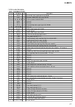
D-NE270

Pin No.

Pin Name

I/O

Description

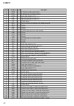
102

MDS

O

Spindle motor drive signal output terminal

103

MDP

O

Spindle motor servo control signal output terminal

104

C176

O

176.4 kHz clock signal output to coil/motor drive

105

VDD2

Power supply terminal (+2.1V)

106

LRCK_O

O

L/R sampling clock signal output to the MP3 decoder

107

LRCK_I

I

L/R sampling clock signal input from the MP3 decoder

108

PCMD_O

O

Serial data output to the MP3 decoder

109

PCMD_I

I

Serial data input from the MP3 decoder

110

BCK_O

O

Bit clock signal output to the MP3 decoder

111

BCK_I

I

Bit clock signal input from the MP3 decoder

112

DVDD

Power supply terminal (+2.1V)

113 to

117

A3 to A0, A10

O

Address signal output to the D-RAM

118 to

120

A11 to A13

O

Not used

Summary of Contents for Walkman D-NE270

Page 1: ...A Japan Electronics and Information Technology Industries Association 2 Recorded at 48 kbps 3 Recorded at 128 kbps 1 Do not play a CD ROM on an audio CD player Operating temperature 5 C 35 C 41 F 95 F Dimensions w h d excluding projecting parts and controls Approx 135 8 30 7 135 8 mm 5 3 8 1 1 4 5 3 8 in Mass excluding accessories Approx 177 g 6 3 oz Design and specifications are subject to change...

Page 2: ...ANUAL OR IN SUPPLEMENTS PUB LISHED BY SONY UNLEADED SOLDER Boards requiring use of unleaded solder are printed with the lead free mark LF indicating the solder contains no lead Caution Some printed circuit boards may not come printed with the lead free mark due to their particular size LEAD FREE MARK Unleaded solder has the following characteristics Unleaded solder melts at a temperature about 40 ...

Page 3: ...s operation the objective lens will move up and down 4 times along with inward motion for the focus search SECTION 1 SERVICING NOTES The laser diode in the optical pick up block may suffer electro static breakdown because of the potential difference generated by the charged electrostatic load etc on clothing and the human body During repair pay attention to electrostatic breakdown and also use the...

Page 4: ...to disable the buttons on the CD player 1 The button has a tactile dot 2 Automatic Music Sensor Display For details see the pages in parentheses 1 Character information display While playing an audio CD disc name track name etc appear on the 2 lines of the display if recorded on the CD While playing an ATRAC CD MP3 CD group name file name etc appear on the 2 lines of the display if recorded on the...

Page 5: ...n below 3 1 DISASSEMBLY FLOW 4 five screws 5 claw 5 two claws 2 two screws 7 flexible flat 20core cable CN801 1 Open the cabinet upper section 8 cabinet lower section 3 Open the battery case lid 5 two claws 6 3 2 CABINET LOWER SECTION Page 5 3 3 OPTICAL PICK UP ASSY CDM 3325ERV Page 6 3 5 LIQUID CRYSTAL DISPLAY PANEL LCD2001 SWITCH BOARD Page 7 SET 3 4 MAIN BOARD Page 6 ...

Page 6: ...ARD 4 OP flexible board CN601 6 optical pick up assy CDM 3325ERV 5 insulator 5 insulator 5 insulator 3 2 two connectors CN401 CN402 1 knob spacer 2 MAIN board 1 Note On installation of main board adjust the position of switch S810 and knob hold knob hold S810 ...

Page 7: ...ISPLAY PANEL LCD2001 SWITCH BOARD 2 eight screws 1 Open the cabinet upper section 3 claw 7 sheet 9 cover 8 SWITCH board 6 liquid crystal display panel LCD2001 CN2001 5 flexible flat 20core cable CN2002 4 Open the cover 3 claw 3 claw ...

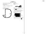
Page 8: ...1 Short SL824 TEST on the MAIN board with a solder bridge Then turn on the power 2 Microcomputer version is displayed on the liquid crystal dis play and the liquid crystal display is all lighted 3 Turn off the power and open the solder bridge on SL824 TEST on the MAIN board Note Remove the solders completely Remaining could be shorted with the chassis etc ...

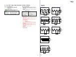
Page 9: ...onnection Procedure 1 Connect the oscilloscope to the test points TP601 RF and TP498 MAIN_GND on the MAIN board 2 Set a disc YEDS 18 3 Push the N X button 4 Check the oscilloscope waveform is as shown below A good eye pattern means that the diamond shape in the center of the waveform can be clearly distinguished RF Signal reference Waveform Eye Pattern VOLT DIV 100 mV With the 10 1 probe in use TI...

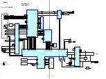
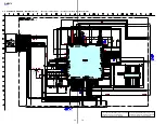
Page 10: ...4 25 XWE 4 XCAS 23 BCK 2 PCMD_O LRCK_O BCK_O PCMD 4 LRCK 1 SK 2 CS 1 XRESET_I 30 DO 4 DI 3 PI3 13 PCMD_I LRCK_I BCK_I PF4 12 18 XRDE PI0 15 PI2 14 D0 D3 17 15 13 11 116 113 117 9 12 15 19 21 8 56 AOUT2 51 AOUT1 61 LRMU RIN 15 LIN 14 MUTE 19 BEEP PWRSW HEADPHONE AMP IC301 17 20 8 LOUT 7 VREF 6 ROUT DC IN 4 5V J401 J301 10 FG_I 90 PWRLAT_O 84 MSDTO0_O 83 MSCK0_O 87 XLAT0_O 85 MSDTI0_I 86 SCOR_I 52 F...

Page 11: ... panel designation A B Line Power voltage is dc 4 5V and fed with regulated dc power supply from DC IN jack J401 Voltages and waveforms are dc with respect to ground in no signal conditions no mark CD PLAY MP3 PLAY Impossible to measure Voltages are taken with aVOM Input impedance 10 MΩ Voltage variations may be noted due to normal produc tion tolerances Waveforms are taken with a oscilloscope Vol...

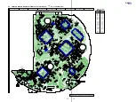
Page 12: ...902 SLED 2 1 M A B C D E F G H I 1 2 3 4 5 6 7 8 9 COMPONENT SIDE MAIN BOARD 15 1 M901 SPINDLE U V W 4 1 OPEN CLOSE DETECT 1 862 996 12 12 5 8 4 1 1 4 OPEN 6 3 PRINTED WIRING BOARD MAIN Board Component Side Uses unleaded solder Semiconductor Location Ref No Location D308 H 3 IC702 A 4 IC803 B 6 Page 18 ...

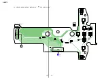
Page 13: ...1 DRY BATTERY SIZE AA IEC DESIGNATION LR6 2PCS 3V A B C D E F G H I 1 2 3 4 5 6 7 8 9 CONDUCTOR SIDE MAIN BOARD TP601 RF 1 10 MAIN_GND 1 862 996 12 12 J301 EXCEPT Canadian 6 4 PRINTED WIRING BOARD MAIN Board Conductor Side Uses unleaded solder D307 H 6 D401 G 3 D402 G 3 D403 H 2 D421 E 5 D422 E 5 IC301 G 7 IC403 G 4 IC601 E 7 IC603 C 8 IC701 B 6 IC801 C 4 IC804 E 4 IC806 B 5 Q408 H 3 Q601 G 7 Semi...

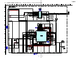
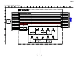
Page 14: ...MSM51X17400F 10TFSR1 470k 100p RF 0 1 22 6 3V 4 7k 100k 10 6 3V 100k 470 10K CXD3039AR 22k 10 6 3V 13 14 15 17 18 19 20 21 22 10 11 9 8 7 6 5 4 3 2 1 RF A B F E OPGSW OPSTB F T T F GFS FOK A B F E RF FRDR FFDR TRDR TFDR SRDR SFDR MDS LRCK_O LRCK_I PCMD_O PCMD_I BCK_O BCK_I A3 A2 A1 A0 A10 A4 A5 A6 A7 A8 A9 XCAS XRAS XWE D1 D0 D3 D2 R8M XRST SCOR SYSM XSDE XLAT SENS DATA CLOK A2 A1 A0 A10 XRAS XWE ...

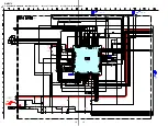
Page 15: ...2 6 3V 0 1 4 7 2 2 2 2 100k 100k TA2120FN EL 10 16V 22k 22k 100p 100p 10 16V 10 0 47 100k XC6206P142MR 4700p UDZSTE 175 1B 24 26 28 29 31 32 34 35 36 37 38 39 40 41 42 43 44 45 46 13 14 15 17 18 19 20 21 22 23 27 PCMD_I LRCK_I BCK_I BCK_O LRCK_O PCMD_O RMKEY REQ_I SDCLK SDOUT SDIN OPEN HOLD BEEP MP3 DECODER SWITCH ON OFF 2 4 1 4V REGULATOR OPEN CLOSE DETECT HOLD ATTSW LIN RIN GND BEEP MUTE PWRSW B...

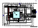
Page 16: ...VDR402 C460 VDR403 VDR401 C415 R413 R438 R480 FB413 R425 1 4P 0 1 1 220k 220 6 3V 10 6 3V 1 1 1M 0 1 2 2M 0 0022 2200p 0 001 100k 100k 0 1 47k 220k 10 6 3V 220 6 3V 4 7 16V 0 1 1 1 4 7 1M 470k 1SS355TE 17 1SS355TE 17 RB160M 30TR TB2138AFG RB160M 30TR 4 7 220 4V 47k 2 2 100k 0 1 10k 47 6 3V 0 001 0 1 0 1 0 001 0 001 470p 1 RB160M 30TR 0 0047 100 47 6 3V 2SB16990LSO 2P 0 1 0 22 22k 10k 1M 1 2 3 4 5 ...

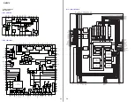
Page 17: ... CONTROL EEPROM 4 4 NOT SUPPLIED RES WR RD LCDA0 D7 D6 D5 D4 D3 D2 D1 D0 VCC2_2 0V VCC3_2 7V DGND AD KEY1 AD KEY2 SGND PS LCD_CS VOL AD7 FOK_I GFS_I CDON_O AUD_SEL DTS_RST_O GND XNMI_I VCPU WAKEUP_K_O TUON_I XRD_O XWR_O LCD_A0 CHG_GND_ON_O EEP_CS_O OPTPWRCTL_O HP_LIN_SEL_I BAT_VCC_O TUPWRON XKRESET_O XCS_O LCD XRST_O XLCD BL_O BOOT XCEX_I MSCK0_O MSDTO0_O MSDTI0_I SCOR_I XLAT0_O XSOE_O VCPU PWRLAT...

Page 18: ...0 18 18 1 860 997 11 11 SWITCH BOARD S2002 2005 S2007 2011 DISPLAY MENU ENTER M m A MAIN BOARD CN801 LCD2001 LIQUID CRYSTAL DISPLAY 24 1 20 1 6 9 PRINTED WIRING BOARD SWITCH Board Uses unleaded solder Page 12 ...

Page 19: ...2018 R2019 R2020 R2021 R2001 S2002 S2007 S2011 S2010 1 1 1 1 24P 20P 2 2k 22k 2 2k 10k 22k 22k 1k 2 2k 4 7k 2 2k 10k 4 7k 0 R2014 0 SGND AD_KEY1 AD_KEY2 DGND VCC2_2 7V PS VCPU_2 0V D0 D1 D2 D3 D4 D5 D6 D7 LCDA0 RD WR LCD_CS RES PS D0 D1 D2 D3 D4 D5 D6 D7 XRES XCS XWR XRD A0 VDD VDD2 VSS VOUT V0 C3 C2 C2 C1 C1 LIQUID CRYSTAL DISPLAY DISPLAY MENU ENTER LCD2001 Page 17 ...

Page 20: ... SPGND U_OUT SPVCC USW VCC0_I VCC1 VCPU VCC2 STNG GSW SEO SEM PREGND INP2 RF2 INM2 LD PD PWG PWS SEP VREF VMMNT_O IMM1 VM3 RO3 PGND3 FO3 VM23 RO2 PGND2 FO2 VM12 R01 RI1 FI1 RI2 FI2 RI3 FI3 PGND1 F01 VM1 DGND ARM77TDMI CPU CORE VIRTUAL ENGINE CORE HUFFMAN HW MAGIC GATE CORE CLOCKGENERATOR SYSTEMCONTROLLER DMAC CH0 DMAC CH1 DMAC CH2 WATCHDOG TIMER PRESCALLER TIME BASETIMER RAM 160K BYTES RAM 512K BY...

Page 21: ...muting on off control signal input from the system controller H muting on 26 WDCK O Not used 27 SCOR O Subcode sync S0 S1 detection signal output to the system controller 28 XRST I Reset signal input from the system controller L reset 29 PWMI I Not used 30 XQOK I Not used 31 XWRE I Not used 32 R8M O System clock output to the system controller 33 VSS0 Ground terminal 34 SQCK I SQSO readout clock s...

Page 22: ...band EFM PLL 79 AVSS3 Ground terminal 80 ASY_O O EFM full swing output terminal 81 ASY_I I Asymmetry comparator voltage input terminal 82 BIAS I Asymmetry circuit constant current input terminal 83 AVDD3 Power supply terminal 2 1V 84 RFAC I EFM signal input from the optical pick up 85 AVDD0 Power supply terminal 2 1V 86 IGEN I Stabilized current input terminal 87 AVSS0 Ground terminal 88 RFDC I RF...

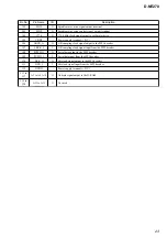
Page 23: ...O O L R sampling clock signal output to the MP3 decoder 107 LRCK_I I L R sampling clock signal input from the MP3 decoder 108 PCMD_O O Serial data output to the MP3 decoder 109 PCMD_I I Serial data input from the MP3 decoder 110 BCK_O O Bit clock signal output to the MP3 decoder 111 BCK_I I Bit clock signal input from the MP3 decoder 112 DVDD Power supply terminal 2 1V 113 to 117 A3 to A0 A10 O Ad...

Page 24: ...IN_I I Serial data input from the MP3 decoder and EEPROM 21 DTS_SDTO O Serial data output terminal Not used 22 DTS_SDTI I Serial data input from terminal Not used 23 DTS_SCK O Serial data transfer clock output terminal Not used 24 AMO_I I Not used 25 VCPU Power supply terminal 2 0V 26 XOUT O Not used 27 GND Ground terminal 28 XIN I System clock signal input from the CD DSP 29 AM1_I I Not used 30 X...

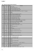
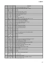
Page 25: ... 74 XLCD BL_O O Not used 75 TYPE1_O O Not used 76 XLED O Not used 77 HP_PWRSW I Power on off control signal output to the headphone amplifier 78 BOOT I Single boot setup terminal 79 XBATT_ICELL_I I Not used 80 NC I Not used 81 XCEX_I I Not used 82 DISPLAY_TYPE I Not used 83 MSCK0_O O Serial data transfer clock output to the CD DSP and power control 84 MSDTO0_O O Serial data output to the CD DSP an...

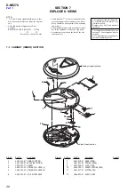
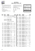
Page 26: ...f No Part No Description Remark 1 3 261 235 01 CABINET UPPER 2 3 261 240 01 LEVER DETECTION 3 3 254 070 11 SCREW 4 3 262 707 01 SPRING FULL OPEN L 5 3 262 708 01 SPRING FULL OPEN R 6 3 261 258 01 LID BATTERY CASE 7 3 261 239 01 KNOB OPEN 8 3 261 251 02 SPRING OPEN 9 3 261 250 01 LOCK OPEN 10 3 034 792 11 SCREW TAPPING B2 0 11 3 261 237 01 BUTTON VOL 12 3 266 622 01 SHEET CDM 7 1 CABINET INNER SECT...

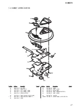
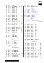
Page 27: ...SPRING BUTTON 56 1 827 979 21 CABLE FLEXIBLE FLAT 20 CORE 57 A 4541 652 A SWITCH BOARD COMPLETE 58 3 260 850 01 COVER 59 3 254 003 01 SCREW 60 3 266 394 01 SHEET COLOR 61 3 260 853 31 ESCUTCHEON 62 3 266 393 02 SHEET PREVENTION STATIC 63 3 266 395 01 SHEET COVER 64 2 025 451 01 CUSHION LCD2001 1 805 467 12 DISPLAY PANEL LIQUID CRYSTAL 7 2 CABINET UPPER SECTION 51 61 52 53 54 64 55 56 62 57 58 59 5...

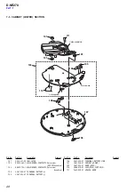
Page 28: ... 1 MAIN BOARD COMPLETE for service Canadian 104 3 261 252 01 TERMINAL BATTERY 105 3 261 253 01 TERMINAL BATTERY 106 3 261 254 01 TERMINAL BATTERY LINK 107 3 261 236 01 CABINET LOWER 108 3 261 238 01 KNOB HOLD 110 3 266 079 01 LEAF PWB COPPER 2 111 3 842 929 01 SPACER KNOB 7 3 CABINET LOWER SECTION 101 101 101 103 110 104 105 106 107 108 main board not supplied CDM 3325ERV 111 Ver 1 1 ...

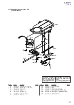
Page 29: ...8 01 RACK 160 3 222 299 01 SPRING RACK RETAINER 161 3 348 998 31 SCREW M1 4X2 5 TAPPING PAN M901 A 3180 953 A MOTOR ASSY TURN TABLE SPINDLE M902 A 3180 951 A MOTOR ASSY SLED 7 4 OPTICAL PICK UP SECTION CDM 3325ERV 151 153 161 160 156 159 158 155 157 151 154 152 M902 M901 Ver 1 1 The components identified by mark 0 or dotted line with mark 0 are critical for safety Replace only with part num ber sp...

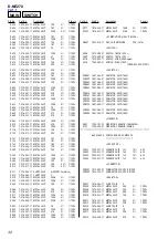
Page 30: ...28 390 11 ELECT CHIP 220uF 20 6 3V C427 1 107 826 11 CERAMIC CHIP 0 1uF 10 16V C428 1 107 686 11 TANTALUM CHIP 4 7uF 20 16V C429 1 164 360 11 CERAMIC CHIP 0 1uF 16V C430 1 162 966 11 CERAMIC CHIP 0 0022uF 10 50V C432 1 126 246 11 ELECT CHIP 220uF 20 4V C433 1 115 156 11 CERAMIC CHIP 1uF 10V C434 1 165 851 11 TANTALUM CHIP 10uF 20 6 3V C435 1 126 205 11 ELECT CHIP 47uF 20 6 3V C436 1 127 688 21 TAN...

Page 31: ...11 FERRITE EMI SMD 2012 FB401 1 216 797 11 METAL CHIP 10 5 1 10W FB402 1 216 797 11 METAL CHIP 10 5 1 10W FB413 1 400 179 21 INDUCTOR EMI FERRITE 1608 FB601 1 414 760 21 FERRITE EMI SMD 1608 FB602 1 414 760 21 FERRITE EMI SMD 1608 FB701 1 414 760 21 FERRITE EMI SMD 1608 FB702 1 414 760 21 FERRITE EMI SMD 1608 IC TRANSISTOR IC301 8 759 681 65 IC AN7531SA IC403 6 704 187 01 IC TB2138AFG IC601 8 752 ...

Page 32: ... 10W R824 1 216 845 11 METAL CHIP 100K 5 1 10W R840 1 216 833 11 METAL CHIP 10K 5 1 10W R866 1 216 833 11 METAL CHIP 10K 5 1 10W R868 1 216 841 11 METAL CHIP 47K 5 1 10W R877 1 216 845 11 METAL CHIP 100K 5 1 10W R886 1 216 845 11 METAL CHIP 100K 5 1 10W R894 1 216 849 11 METAL CHIP 220K 5 1 10W R903 1 216 821 11 METAL CHIP 1K 5 1 10W R935 1 216 845 11 METAL CHIP 100K 5 1 10W R942 1 216 841 11 META...

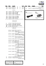
Page 33: ...OLISH RUSSIAN East European 2 023 885 61 MANUAL INSTRUCTION CZECH SLOVAKIAN East European 2 023 891 01 CARD EXPLANATION AEP 3 265 088 11 MANUAL INSTRUCTION Installation operation guide ENGLISH 3 265 088 21 MANUAL INSTRUCTION Installation operation guide SPANISH FRENCH PORTUGUESE EXCEPT East European 3 265 088 31 MANUAL INSTRUCTION Installation operation guide GERMAN ITALIAN DUTCH AEP 3 265 088 41 ...

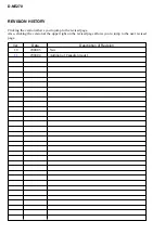
Page 34: ...rsion allows you to jump to the revised page Also clicking the version at the upper right on the revised page allows you to jump to the next revised page Ver Date Description of Revision 1 0 2004 03 New 1 1 2004 04 Addition of Canadian model ...

Reviews: