background image

http://cxema.ru

– 21 –

KV-XG29N90

RM-915

2-9.

A AND B6 BO

ARDS REMO

V

A

L

2-8.

H2 BO

ARD REMO

V

A

L

3

 Two connectors

4

 One screw (+BVTAP 3 

×

 12)

1

 Two connectors

4

 Four claws

5

 H2 Board

2

 Two connectors

4

 B6 Board  

5

 A Board

1

 Two screws

     (+BVTAP 3 

× 

12)

2

 Two screws

     (+BVTAP 3 

× 

12)

2-10

PICTURE 

TUBE REMO

V

A

L

Note:

 The 

picture 

tube 

for 

New 

Zealand 

model 

is 

upside 

do

wn,

and 

the 

position 

for 

anode 

cap 

and 

tension 

spr

ing 

are 

changed

accordingly

.

!

F

our DGC clips

Degaussing coil

0

F

our cla

ws

1

Four scre

ws 

(+BVTP 3 

× 

16)

2

Speaker Bracket

assy (L)

5

Speaker Bracket

assy (R)

Two screws

(Tapping)

6

Chassis assy

9

Deflection

yo

ke

8

Nec

k assy

7

C6 board

5

Anode cap

!

Picture tube

Cushion

Two screws

(Tapping)

T

ension

spr

ing

3

Eight scre

ws 

(+BVTP 4 

× 

16)

4

Eight scre

ws 

(+BVTP 4 

× 

16)

6

Four scre

ws 

(+BVTP 3 

× 

16)

DGC holder

DGC holder

Cushion (50 

× 

550) 

DGC

Cushion (50 

× 

550) 

DGC

Summary of Contents for Trinitron KV-XG29N90

Page 1: ...http cxema ru MODEL COMMANDER DEST CHASSIS NO KV XG29N90 RM 915 Taiwan SCC P13K A MODEL COMMANDER DEST CHASSIS NO CHASSIS TRINITRON COLOR TV SERVICE MANUAL BG 3S ...

Page 2: ... input lines available 2 Headphone Output 1 Minijack Picture tube 29 inch Tube size cm 72 Measured diagonally Screen size cm 68 Measured diagonally Dimension w h d mm 794 573 517 Mass kg 48 Design and specifications are subject to change without notice SAFETY RELATED COMPONENT WARNING COMPONENTS IDENTIFIED BY SHADING AND MARK ON THE SCHEMATIC DIAGRAMS EXPLODED VIEWS AND IN THE PARTS LIST ARE CRITI...

Page 3: ... 26 3 4 G2 Screen and White Balance Adjustments 27 4 CIRCUIT ADJUSTMENT 4 1 Adjustments with Commander 28 4 2 Adjustment Method 29 4 3 Picture Quality Adjustments 34 4 4 A Board Adjustment After IC003 Memory Replacement 34 4 5 Picture Distortion Adjustment 35 Section Title Page 5 DIAGRAMS 5 1 Block Diagram 37 5 2 Frame Schematic Diagram 40 5 3 Circuit Boards Location 43 5 4 Schematic Diagrams and ...

Page 4: ...Detected Symptoms Power does not come on No power is supplied to the TV AC power supply is faulty Power does not come on Load on power line is shorted Has entered standby state after horizontal raster Vertical deflection pulse is stopped Power line is shorted or power supply is stopped No raster is generated CRT cathode current detection reference pulse output is small Power is shut down shortly a...

Page 5: ...al deflection stopped White balance failure 5 times One flash count is not used for self diagnostic 3 STOPPING THE STANDBY TIMER FLASH Turn off the power switch on the TV main unit or unplug the power cord from the outlet to stop the STANDBY TIMER lamp from flashing STANDBY SLEEP lamp Lamp ON 0 3 sec Lamp OFF 3 sec Lamp OFF 0 3 sec 2 times 5 times ...

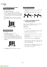
Page 6: ...results displayed on the screen are not automatically cleared always check the self diagnostic screen during repairs When you have completed the repairs clear the result display to 0 Unless the result display is cleared to 0 the self diagnostic function will not be able to detect subsequent faults after completion of the repairs Clearing the result display To clear the result display to 0 press bu...

Page 7: ...ed by Q509 and IC001 shut down the power supply Vertical deflection overcurrent Occurs when an overcurrent on V drive line is detected by Q507 Power supply will be shut down when detect this by IC001 White balance failure If the RGB levels do not balance or become low level within 5 seconds this error will be detected by IC301 TV will stay on but there will be no picture Refers to the RGB levels o...

Page 8: ...te Remove F Bracket first SECTION 2 DISASSEMBLY 2 3 CHASSIS ASSY REMOVAL 2 2 SPEAKER REMOVAL 2 1 REAR COVER REMOVAL 2 Eight screws BVTP 4 16 3 Three screws BVTP 4 16 1 Rear cover 1 Eight screws BVTP 4 16 3 Four screws BVTP 3 16 2 Bracket speaker 1 Chassis assy ...

Page 9: ... Control Button and Light Guide unscrew them exchange with the new parts and fix them with screws BVTP respectively 2 5 1 REPLACEMENT OF CONTROL BUTTON 2 6 D3 BOARD REMOVAL Control button Two screws BVTP 3 12 One screw BVTP 3 12 1 Three connectors 2 One claw 3 D3 board 3 Two claws 4 Terminal bracket 1 Two screws BVTP 3 12 2 One screw BVTP 4 16 ...

Page 10: ... New Zealand model is upside down and the position for anode cap and tension spring are changed accordingly Four DGC clips ª Degaussing coil 0 Four claws 1 Four screws BVTP 3 16 2 Speaker Bracket assy L 5 Speaker Bracket assy R Two screws Tapping 6 Chassis assy 9 Deflection yoke 8 Neck assy 7 C6 board 5 Anode cap Picture tube Cushion Two screws Tapping Tension spring 3 Eight screws BVTP 4 16 4 Eig...

Page 11: ...A metal fitting called the shatter hook terminal is built into the rubber 3 Do not turn the foot of rubber over too hard The shatter hook terminal will stick out or damage the rubber HOW TO HANDLE AN ANODE CAP 3 When one side of the rubber cap is separated from the anode button the anode cap can be removed by turning up the rubber cap and pulling it up in the direction of the arrow c 2 Using a thu...

Page 12: ...he pattern generator Contrast Brightness 2 Position neck assy as shown in Fig3 2 3 Set the pattern generator raster signal to a green raster 4 Move the deflection yoke to the rear and adjust with the purity control so that the green is at the center and the blue and the red take up equally sized areas on each side See Figures 3 1 through 3 4 5 Move the deflection yoke forward and adjust so that th...

Page 13: ...nd blue dots are on top of each other at the center of the screen 3 If the H STAT variable resistor cannot bring the red green and blue dots together at the center of the screen adjust the horizontal convergence with the H STAT variable resistor and the V STAT magnet in the manner given below In this case the H STAT variable resistor and the V STAT magnet influence each other so be sure to perform...

Page 14: ...nets should be equally far from the horizontal center line 2 Do not separate the Red and Blue magnets too far Less than 8 mm 2 Dynamic Convergence Adjustment Preparation Before starting this adjustment adjust the horizontal static convergence and the vertical static convergence 4 BMC Hexapole Magnet If the red green and blue dots are not balanced or aligned then use the BMC magnet to adjust in the...

Page 15: ...US control on the flyback transformer for the best focus FLYBACK TRANSFORMER T503 TLV Rotate TLV 2 VOL 29 34 on DY Rotate TLV VOL 25 on DY XCV Rotate XCV Adj core on DY YCH Rotate YCH VOL on DY TLH Insert TLH Correction Plate to DY Pocket Left or Right ON DY YCH XCV TLV1 TLV2 b a c d a d screen corner misconvergence a b c d Permalloy assembly Screen Focus ...

Page 16: ...RIGHT ADJUSTMENT 1 Set to service mode 2 Input a staircase signal of black to white from the pattern generator 3 BRIGHTNESS 50 PICTURE MINIMUM 4 Select SBR WHB7 with 1 and 4 and adjust SBR WHB7 level with 3 and 6 so that the second stripe from the right is dimly lit 3 4 G2 SCREEN AND WHITE BALANCE ADJUSTMENTS 1 G2 SCREEN ADJUSTMENT 1 Set the PICTURE to normal 2 Put to VIDEO input mode without sign...

Page 17: ... the commander then press POWER button again hereupon it becomes TV mode c METHOD OF WRITE INTO MEMORY 1 Set to Service Mode 2 Press 1 UP and 4 DOWN select an item of adjustment 3 Press MUTING button and it will indicate WRITE on the screen 4 Press 0 button to write into memory d MEMORY WRITE CONFIRMATION METHOD 1 After adjustment pull out the plug from AC outlet and then plug into AC outlet again...

Page 18: ...k to SERVICE Use the same method for all Items Use 1 and 4 to select the adjustment item use 3 and 6 to adjust write with MUTING then execute the write with Note 1 In WRITE the data for all items are written into memory together 2 For adjustment items that have different standard data between 50Hz or 60Hz be sure to use the respective input signal after adjustment 1F SERVICE 50 HPS Adjusted with 3...

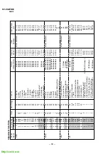
Page 19: ... G Drive DYNAMIC others 0A 7 2 90 7 2 2 BDR 2A 3F B Drive DYNAMIC others 0B 7 2 91 7 2 3 RCT 7 0F R Cutoff SECAM others 07 3 0 93 3 0 4 GCT 7 0F G Cutoff SECAM others 08 7 4 94 7 4 5 BCT 7 0F B Cutoff SECAM others 08 3 0 94 3 0 6 BMN 15 1F Brightness Minimum Data 97 7 SBR 28 3F Sub Brightness Control 98 SAJ 0 PMX 33 3F Picture Maximum Data CXA2139S 88H 96 1 SHU 8 0F Sub Hue Control TV Video 99 2 S...

Page 20: ... 0 3 PH2 0 3 Phase 2 Register Selection 76 3 2 4 PH3 0 3 Phase 3 Register Selection 76 5 4 5 PH4 0 3 Phase 4 Register Selection 76 7 6 6 BCS 2 3 Bass Center Shift 4 3 0 1A8 1 0 7 TCS 2 3 Treble Center Shift 5 3 0 1A9 1 0 8 TRF 2 3 RF Treble Offset 5 3 0 1A9 5 4 MSP 0 WST 15 FF W G Stereo Threshold MSP3415D 84H 157 7 0 1 WBT EA FF W G Bilingual Threshold 158 7 0 2 WLL 5 FF W G Monaural Threshold 15...

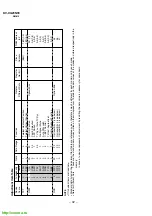
Page 21: ...s Device Functionality Note Data Range Function Note for Register Slava RAM Address Name No Name Different Data No bit Address bit TXT 0 TXH 1 3 Teletext Horizontal Position 58H 18D 1 0 1 TXV 0 3 Teletext Vertical Position 18D 6 4 OPM 0 OSH 0A 3F OSD H Position Option Misc AC 7 2 1 COM 0 03 Comb Selection A5 7 6 2 APC 1 1 APC Switch A4 5 3 TSY 0 03 TV Sys at Auto TV Sys A4 4 3 4 MUT 0 1 No Signal ...

Page 22: ...ang 1 SECAM 1 XTAL 3 58 1 XTAL 4 43 1 ITEM INFORMATION No OPB0 OP1 No OPB1 OP2 No OPB2 OP3 Item KV XG29N90 1 1 DVD Input 0 Dis Fav 0 Thai Bil 0 HDEV 1 NICAM 0 TOP 0 Item KV XG29N90 Color SW 0 11 KEY 0 AV Mono 1 US ST 0 Auto TV sys 0 Auto PIC 1 2199 Curve 0 PIC Rotate 1 AV Input ...

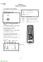
Page 23: ...der to write the data BELL FILTER ADJUSTMENT 1 Input SECAM color bar signal 2 Connect the dual trace oscilloscope to CN303 pin 9 not mounted 3 Adjust SERVICE MODE ITEMS SBF as shown below 4 4 A BOARD ADJUSTMENT AFTER IC003 MEMORY REPLACEMENT When replacing IC003 MEMORY be sure to change IC001 µ COM to the following new IC at the same time IC001 µ CON CXP86449 618S 1 Enter to Service Mode 2 Press c...

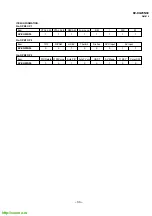
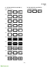
Page 24: ...TION ADJUSTMENT 2 GEO 0 HPS H POSITION GEO 1 HSZ H SIZE GEO 2 PAP PIN AMP GEO 5 VSZ V SIZE GEO 7 VLN V LINEARITY GEO 4 VPS V POSITION GEO 6 SCO VERTICAL S Correction GEO 8 BOW AFC BOW GEO 9 AGL AFC ANGLE GEO 3 TLT TRAPEZIUM GEO 0A UCP UPPER CORNER PIN GEO 0B LCP LOWER CORNER PIN H TRAPEZOID Rotate RV1801 ...

Page 25: ...http cxema ru 36 KV XG29N90 RM 915 MEMO ...

Page 26: ...V OUT IC503 TDA8172 HDT T501 H DRIVE Q506 2SC2688 PIN CONT IC502 NJM2903M PIN OUT Q505 IRF614 PMT T505 HLT T504 FBT T503 NX 4009 V PARA IC2801 DQP V DRIVE Q2802 2803 2804 DQP H DRIVE Q2801 DF TRANS T2800 B Audio Front Vcc 9V 11V 7V 5V 5V REG RESET IC002 MM1319AF 9V REC IC603 5V REC IC604 STB TRANS T604 STB SW TR Q605 2SK2845 SRT T603 POWER IC601 STR F6656 LINE FILTER T601 LINE FILTER T8601 T8602 T...

Page 27: ...ICRO CN701 3P MINI CN700 1P TAB CN702 1P RGB OUT CN706 1P TAB CN704 1P TAB N S COIL NC GND GND TO DGC TO DY HV G4 G1 KR G2 KB KG CV H QP Q P Q P E VM QP VM DY C6 DQP DYNAMIC FOCUS D3 H DY H DY V DY V DY V R L 2 1 J3901 J3902 J3903 3P 4 3 TO SPEAKER 1 NS MUTE NS ROT 15V VD GND VD 2 3 4 5 6 1 H H H H V V 2 3 4 5 6 1 B G R GND IK 9V 2 3 4 5 6 1 B G R GND IK 9V 2 3 4 5 6 1 200V E H1 2 3 1 200V GND H1 ...

Page 28: ...ngs are taken with a 10 M Ω digital multimeter Voltage are dc with respect to ground unless other wise noted Voltage variations may be noted due to normal pro duction tolerances All voltages are in V Cannot be measured Circled numbers are waveform references B bus B bus signal path Reference information RESISTOR RN METAL FILM RC SOLID FPRD NONFLAMMABLE CARBON FUSE NONFLAMMABLE FUSIBLE RS NONFLAMMA...

Page 29: ...D203 C 11 D300 A 9 D301 B 9 D302 B 6 D303 B 5 D304 B 5 D305 B 5 D306 C 5 D307 C 5 D308 B 5 D309 B 6 D310 A 6 D311 C 6 D312 C 6 D313 A 8 D315 B 7 D316 C 7 D317 B 9 D314 A 9 D319 C 7 D320 C 6 D321 B 6 D322 B 6 D401 D 2 D402 C 3 D403 B 2 D404 C 2 D405 C 1 D406 B 1 D407 C 2 D408 C 1 D409 A 1 D504 D 5 D505 H 6 D506 F 6 D507 F 6 D508 I 5 D509 F 6 D510 F 5 D511 F 5 D512 G 5 D513 I 5 D517 F 2 D518 F 2 D51...

Page 30: ...P 470 CHIP 0 CHIP 6P WHT S MICRO 10k CHIP 0 CHIP CHIP 100 CHIP 0 1 25V B CHIP 220 CHIP 18p CH CHIP 18k CHIP 3 9k CHIP 3 9k CHIP 3 9k CHIP 10p CH CHIP 10p CH CHIP 10p CH CHIP 100 CHIP 4 7k CHIP 4 7 k CHIP 4 7k CHIP 4 7 k CHIP 100 CHIP 0 1 25V B CHIP 0 1 25V B CHIP 1k CHIP 4 7k CHIP 10k CHIP 0 022 B CHIP 1M CHIP 10k CHIP 47p CH CHIP JW 5mm 10k CHIP 10k CHIP 470p B CHIP CHIP 100 CHIP 1k CHIP CHIP 1k ...

Page 31: ...SS355 10k CHIP 27k CHIP 100p CH CHIP 0 CHIP 100k 100 10V RS3FS DAMPER RS3FS DAMPER 2P VH 2P MINI 7P YEL S MICRO EL0606 5 6k 1W RS 470k RN CHIP 0 CHIP 1000 25V 0 1 250V 0 15 250V PP 220 RN CP 2 2k RN CP 3 9k RN CP 3 9k RN C P 8 2k RN CP 10k RN CP 22k RN CP 39k RN CP 100k RN CP 39k RN CP 4 7k RN CP 1k 3W RS 2SD2578 CA H OUT 2SC2688 H DRIVE 680 3W RS JW 7 5 JW 5MM 8 2M 1W 6 8 10W RB 7 5MM 7 5MM 1 5mH...

Page 32: ...7 3 23 0Vp p H PAL SECAM 135V 3 3Vp p H NTSC 13 6Vp p H 3 3Vp p H PAL SECAM 135Vp p H 3 3Vp p H NTSC 15 0Vp p H PAL SECAM 144Vp p H 3 BLUE CATHODE CURRENT RED CATHODE CURRENT GREEN CATHODE CURRENT VDD VDD BLUE INPUT GREEN INPUT RED INPUT RED FEEDBACK GREEN FEEDBACK BLUE FEEDBACK RED OUTPUT GREEN OUTPUT BLUE OUTPUT GROUND GND REFERENCE VOLTAGE D 3 Board DOP DYNAMIC FOCUS D 3 PRINTED WIRING BOARD ...

Page 33: ... 1k 5 6k JW 5MM 3 3k 47k 100k 1 2W 4 7 250V 100 FPRD 2SC2785 G AMP 1SS119 PROTECT 100 FPRD 1SS119 PROTECT 1SS119 PROTECT 1SS119 PROTECT 1SS119 PROTECT 1SS119 PROTECT 1SS119 PROTECT 1SS119 PROTECT 1SS119 PROTECT 1SS119 PROTECT 1SS119 PROTECT 1SS119 PROTECT 1SS119 PROTECT 1SS119 PROTECT 2SC2611 B OUT 2SC2611 G OUT 2SC2611 R OUT 2SA1091 B IK DETECT 47 47 47 4 7k 33k 1SS119 PROTECT 1SS119 PROTECT 100 ...

Page 34: ...V IN Y IN S Y C CN904 CN104 CN601 TO A BOARD TO A BOARD TO A BOARD TO A BOARD TO B6 BOARD TO B6 BOARD CN901 CN8403 CN8602 TO SP 0 1 0 1 4 9 1 2 1 3 CONTROL PANEL 7V 5V 5V 5V AUDIO L AUDIO R 4 8 4 8 4 8 B SSSBG3S H2 AUDIO R Y S AUDIO L AUDIO R C Y S 1 2 3 4 5 6 7 1 2 3 4 5 6 7 8 1 2 3 C5903 C5907 C5908 C5912 C5914 C5917 CN5901 D5901 D5903 D5905 R5913 R5921 R5924 R5929 C5904 C5915 R5928 L5901 CN5904...

Page 35: ...c diagrams H 2 VM 1 boards KV XG29N90 RM 915 KV XG29N90 RM 915 KV XG29N90 RM 915 KV XG29N90 RM 915 B 6 Board B 6 CISPR A C FUSE AV INPUT MONITOR INPUT VM 1 Board H 2 CONTROL PANEL PRINTED WIRING BOARDS H 2 Board VELOCITY MODULATION VM 1 ...

Page 36: ...IP 100 CHIP 10k CHIP 39k CHIP 39k CHIP 470 CHIP 2 2k CHIP 680 CHIP 3 9k CHIP 10k CHIP 1k CHIP 10k CHIP 1k CHIP 470k CHIP 470 CHIP 68 CHIP 470k CHIP 470k CHIP 47k CHIP 47k CHIP 470k CHIP 75 CHIP 15k CHIP 470k CHIP 75 CHIP 220 CHIP 220 CHIP 47k CHIP 470k CHIP 47k CHIP RD9 1SB T1 RD9 1SB T1 47 3 3k CHIP 22k CHIP 10k CHIP 0 1 25V B CHIP 220 CHIP 150p CH CHIP 1k CHIP 0 1 F CHIP 1k CHIP 0 1 F CHIP 10k C...

Page 37: ...B1 T1 RD9 1S B UDZS TE17 5 1B UDZS TE17 9 1B 1SS355TE 17 5P6M DA204K DAP202K AK04V0 AU 01Z V1 D2L20U EL1Z ERA22 08 GP08D NNCD9 1A T1 RD33EB3T RGP02 17EL 6433 ERC04 06SE RN4Z RS3FS RU4AM T4 31DQ06 FC5 D1NS4 D1N20R HZS9 1NB2 RD39ES B2 RD20ES B2 RD30ESB2 RD6 8ES B1 1SS119 25 D3SB60 TRANSISTOR E C B 5 5 SEMICONDUCTORS DIODE CATHODE ANODE CATHODE ANODE CATHODE ANODE SPB 26MVWF CATHODE ANODE GRN ANODE G...

Page 38: ... part number and no description are not stocked because they are seldom required for routine service The construction parts of an assembled part are indicated with a collation number in the remark column REF NO PART NO DESCRIPTION REMARK 6 1 SPEAKER BRACKET p 7 685 663 71 SCREW BVTP 4 16 r 7 685 648 79 SCREW BVTP 3 12 1 4 071 045 02 BRACKET SPEAKER 2 4 054 981 01 SCREW STEP TAPPING 3 1 529 563 11 ...

Page 39: ...MPLETE 53 4 022 115 00 HOLDER AC CORD 54 1 575 023 21 CORD POWER WITH CONNECTOR 7 5A 250V 55 4 066 684 72 BRACKET TERMINAL 56 4 046 797 01 SCREW 3X12 BVTAP 57 A 1299 323 A A BOARD COMPLETE 58 1 453 284 11 TRANSFORMER ASSY FLYBACK NX 4009 M3I4 59 4 066 681 12 BRACKET MAIN 60 A 1343 763 A D3 BOARD MOUNTED 61 8 598 477 10 TUNER FSS BTF WG411 54 57 55 58 56 53 60 59 51 52 61 ...

Page 40: ...R HV CABLE 114 4 046 600 11 SPACER DY 115 4 077 228 01 PIECE PLT CONVENGENCE REF NO PART NO DESCRIPTION REMARK 116 8 451 494 31 DEFLECTION YOKE Y29RSA S 117 8 453 011 11 NA299 M 118 A 1332 011 A C6 BOARD MOUNTED 119 1 419 519 11 COIL DEMAGNETIC 120 4 062 970 11 CLIP 29RSN DGC 121 1 452 896 11 COIL NA ROTATION RT200 122 A 1342 519 A VM1 BOARD MOUNTED 123 4 369 318 61 SPRING TENSION 124 1 452 032 00...

Page 41: ... 126 965 11 ELECT 22UF 20 00 50V C209 1 126 965 11 ELECT 22UF 20 00 50V C210 1 126 933 11 ELECT 100UF 20 00 16V C211 1 126 941 11 ELECT 470UF 20 00 25V C212 1 126 933 11 ELECT 100UF 20 00 16V C213 1 126 933 11 ELECT 100UF 20 00 16V C214 1 126 942 61 ELECT 1000UF 20 00 25V C215 1 126 942 61 ELECT 1000UF 20 00 25V C216 1 163 021 91 CERAMIC CHIP 0 01UF 10 00 50V C217 1 126 964 11 ELECT 10UF 20 00 50V...

Page 42: ...6 1 102 244 00 CERAMIC 220PF 10 00 500V C567 1 115 520 11 FILM 0 68UF 5 00 250V C568 1 102 228 00 CERAMIC 470PF 10 00 500V C570 1 115 522 11 FILM 1UF 5 00 250V C572 1 117 661 21 FILM 0 15UF 5 00 250V C573 1 106 387 00 MYLAR 0 068UF 10 00 200V C574 1 104 709 11 ELECT 4 7UF 160V C576 1 130 495 00 MYLAR 0 1UF 5 00 50V C577 1 106 395 00 MYLAR 0 15UF 10 00 200V C582 1 164 004 11 CERAMIC CHIP 0 1UF 10 0...

Page 43: ...7 9 1B D321 8 719 069 60 DIODE UDZS TE17 9 1B D322 8 719 069 60 DIODE UDZS TE17 9 1B D504 8 719 302 43 DIODE EL1Z D505 8 719 988 61 DIODE 1SS355TE 17 D506 8 719 911 19 DIODE 1SS119 25TD D507 8 719 988 61 DIODE 1SS355TE 17 D508 8 719 988 61 DIODE 1SS355TE 17 D509 1 216 073 00 RES CHIP 10K 5 1 10W D510 8 719 988 61 DIODE 1SS355TE 17 D511 8 719 988 61 DIODE 1SS355TE 17 D512 8 719 988 61 DIODE 1SS355T...

Page 44: ... SHORT 0 JR502 1 216 295 11 SHORT 0 JR503 1 216 295 11 SHORT 0 JR600 1 216 295 11 SHORT 0 COIL L002 1 414 856 11 INDUCTOR 10UH L003 1 414 180 11 INDUCTOR 3 3UH L005 1 414 233 22 INDUCTOR CHIP 0UH L101 1 414 856 11 INDUCTOR 10UH L102 1 414 856 11 INDUCTOR 10UH L103 1 414 856 11 INDUCTOR 10UH L104 1 414 856 11 INDUCTOR 10UH L105 1 414 856 11 INDUCTOR 10UH L301 1 414 189 31 INDUCTOR 100UH L302 1 414 ...

Page 45: ...ES CHIP 27K 5 1 10W R040 1 216 025 11 RES CHIP 100 5 1 10W R041 1 216 025 11 RES CHIP 100 5 1 10W R042 1 216 295 11 SHORT 0 R043 1 216 049 11 RES CHIP 1K 5 1 10W R044 1 216 025 11 RES CHIP 100 5 1 10W R045 1 414 233 22 INDUCTOR CHIP 0UH R046 1 216 049 11 RES CHIP 1K 5 1 10W R047 1 414 233 22 INDUCTOR CHIP 0UH R048 1 216 073 00 RES CHIP 10K 5 1 10W R050 1 216 073 00 RES CHIP 10K 5 1 10W R053 1 216 ...

Page 46: ...0 5 2W R590 1 215 465 00 METAL 68K 1 1 4W R591 1 260 288 11 CARBON 0 47 5 1 2W R592 1 208 820 11 METAL CHIP 39K 0 5 1 10W R593 1 260 288 11 CARBON 0 47 5 1 2W R594 1 260 288 11 CARBON 0 47 5 1 2W R595 1 216 073 00 RES CHIP 10K 5 1 10W R315 1 216 053 00 RES CHIP 1 5K 5 1 10W R316 1 216 053 00 RES CHIP 1 5K 5 1 10W R317 1 216 077 91 RES CHIP 15K 5 1 10W R318 1 216 051 00 RES CHIP 1 2K 5 1 10W R319 1...

Page 47: ...DE 0 22 5 2W R640 1 249 415 11 CARBON 680 5 1 4W R641 1 216 361 21 METAL OXIDE 0 22 5 2W R642 1 249 419 11 CARBON 1 5K 5 1 4W R643 1 247 843 11 CARBON 3 3K 5 1 4W R644 1 249 419 11 CARBON 1 5K 5 1 4W R646 1 215 924 00 METAL OXIDE 15K 5 3W R647 1 249 387 11 CARBON 3 3 5 1 4W R648 1 216 057 00 RES CHIP 2 2K 5 1 10W R649 1 249 417 11 CARBON 1K 5 1 4W R650 1 215 882 00 METAL OXIDE 22 5 2W R652 1 215 9...

Page 48: ...C8407 1 164 346 11 CERAMIC CHIP 1UF 16V C8408 1 163 133 00 CERAMIC CHIP 470PF 5 00 50V C8409 1 126 933 11 ELECT 100UF 20 00 16V C8410 1 164 346 11 CERAMIC CHIP 1UF 16V C8411 1 163 133 00 CERAMIC CHIP 470PF 5 00 50V C8412 1 164 346 11 CERAMIC CHIP 1UF 16V C8413 1 163 133 00 CERAMIC CHIP 470PF 5 00 50V C8414 1 126 963 11 ELECT 4 7UF 20 00 50V C8415 1 163 133 00 CERAMIC CHIP 470PF 5 00 50V C8416 1 16...

Page 49: ... 10K 5 1 10W R8403 1 216 073 00 RES CHIP 10K 5 1 10W R8404 1 216 073 00 RES CHIP 10K 5 1 10W R8405 1 216 049 11 RES CHIP 1K 5 1 10W R8406 1 216 073 00 RES CHIP 10K 5 1 10W R8407 1 216 049 11 RES CHIP 1K 5 1 10W R8408 1 216 049 11 RES CHIP 1K 5 1 10W R8409 1 216 041 00 RES CHIP 470 5 1 10W R8410 1 216 113 00 RES CHIP 470K 5 1 10W R8411 1 216 113 00 RES CHIP 470K 5 1 10W R8412 1 216 041 00 RES CHIP ...

Page 50: ...11 8 719 911 19 DIODE 1SS119 25TD D712 8 719 911 19 DIODE 1SS119 25TD D713 8 719 911 19 DIODE 1SS119 25TD D714 8 719 911 19 DIODE 1SS119 25TD D715 8 719 911 19 DIODE 1SS119 25TD D716 8 719 911 19 DIODE 1SS119 25TD D717 8 719 929 15 DIODE RD9 1ES T1B D1803 8 719 911 19 DIODE 1SS119 25TD D1804 8 719 911 19 DIODE 1SS119 25TD D1808 8 719 908 03 DIODE GP08D IC IC1800 8 759 822 38 IC LA6510 JACK J701 1 ...

Page 51: ...1825 1 247 843 11 CARBON 3 3K 5 1 4W VARIABLE RESISTOR RV702 1 241 656 11 RES ADJ METAL FILM 110M RV1801 1 238 019 11 RES ADJ CARBON 47K A 1343 763 A D3 BOARD MOUNTED CAPACITOR C2800 1 104 664 11 ELECT 47UF 20 00 25V C2801 1 106 220 00 MYLAR 0 1UF 10 00 100V C2802 1 136 155 00 FILM 0 015UF 5 00 50V C2803 1 129 723 00 FILM 0 056UF 5 00 630V C2805 1 104 664 11 ELECT 47UF 20 00 25V C2806 1 106 383 00...

Page 52: ... 1 249 426 11 CARBON 5 6K 5 1 4W R2908 1 249 413 11 CARBON 470 5 1 4W R2909 1 249 417 11 CARBON 1K 5 1 4W R2910 1 249 420 11 CARBON 1 8K 5 1 4W R2911 1 249 411 11 CARBON 330 5 1 4W R2912 1 247 843 11 CARBON 3 3K 5 1 4W R2913 1 249 429 11 CARBON 10K 5 1 4W R2914 1 249 411 11 CARBON 330 5 1 4W R2915 1 249 429 11 CARBON 10K 5 1 4W R2916 1 249 401 11 CARBON 47 5 1 4W R2920 1 247 807 31 CARBON 100 5 1 ...

Page 53: ...5 1 4W R5912 1 249 437 11 CARBON 47K 5 1 4W R5914 1 249 403 11 CARBON 68 5 1 4W R5915 1 249 429 11 CARBON 10K 5 1 4W R5916 1 249 419 11 CARBON 1 5K 5 1 4W R5917 1 249 416 11 CARBON 820 5 1 4W R5918 1 249 429 11 CARBON 10K 5 1 4W R5919 1 249 417 11 CARBON 1K 5 1 4W R5920 1 249 439 11 CARBON 68K 5 1 4W R5921 1 216 476 11 METAL OXIDE 180 5 3W R5922 1 249 414 11 CARBON 560 5 1 4W R5923 1 249 383 11 CA...

Reviews: